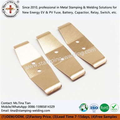


Pressing Copper Stamping Bending Connecting Parts
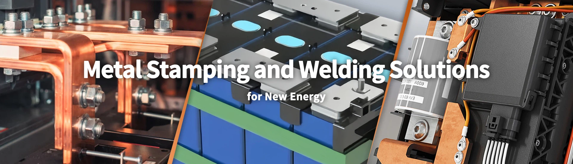
Pressing Copper Stamping Bending Connecting Parts are precision-customized components made of copper and copper alloys as base materials, and formed in one piece through two core cold working processes: pressing and bending. They are mainly used in industrial scenarios such as electric vehicles (EVs), energy storage systems (ESS), power distribution equipment, and electronic devices. They undertake the core functions of component connection, fixation, and electrical signal/current transmission, and are a key intermediate link between copper base material processing and mass production of terminal equipment.
- Fast Delievery
- Quality Assurance
- 24/7 Customer Service
Product Introduction

Pressing Copper Stamping Bending Connecting Parts are metal parts made by precision stamped of high-purity copper into specific bending angles and connection structures. They are designed to provide highly conductive and fatigue-resistant electrical connections for power transmission systems (such as battery modules and inverters) and precision electronic equipment.
Working principle
Stamping Forming Principle
At room temperature, a pressure of 50-500 MPa is applied to the copper substrate using a stamping die, causing plastic deformation and forming the component according to the die. The stamping speed is controlled at 10-50 mm/s, ensuring a dimensional error within ±0.01-±0.05 mm, forming the basic structure of the connector.
Bending Forming Principle
Building upon stamping, a specialized die is used to bend the copper material to a customizable angle of 0-180°. The bending radius is controlled to be no less than 1.5 times the copper thickness, and the bending force is controlled to prevent deformation and cracking, ensuring the strength and stability of the bent part.
Connection and Conduction Principle
The formed connector achieves a tight connection with various electrical components through its own interface, contacts, or fixed structure. Utilizing the excellent conductivity of copper, it efficiently transmits electrical signals and high currents, ensuring a strong connection, low loss, and stable equipment operation.

Surface treatment
Tin plating
0.5-2μm thickness, improves solderability, prevents copper oxidation, suitable for applications requiring soldering connections (e.g., circuit board interfaces) for Copper Stamping Spring Contacts for Electrical Switch.
Silver plating
0.1-1μm thickness, excellent conductivity and low contact resistance, suitable for high-frequency, low-signal transmission applications (e.g., precision electronic device connections) for Copper Metal Stamping Electrical Silver Contact Parts.
Nickel plating
1-3μm thickness, improves corrosion resistance and surface hardness, suitable for outdoor, corrosive environments (e.g., photovoltaic inverter connections) for Copper Stamping.
Ultrasonic cleaning
Utilizes high-frequency ultrasonic oscillation for deep cleaning of copper surfaces, effectively removing oil, oxide layers, and impurities, preventing oxidation and rust during subsequent use. Suitable for general industrial applications and at a lower cost.

Frequently Asked Questions
What is the impact of bending radius on electrical performance?
+
-
A bending radius that is too small (<1.5 times the material thickness) can cause copper grain fracture, leading to a 20%-30% increase in resistance. It is recommended to use a design with R≥2T (T=material thickness) and verify internal cracks using X-ray inspection.
What is the typical contact resistance of stamped and bent copper contacts? How can this be guaranteed?
+
-
Under normal pressure (15~30N) and tin plating conditions, the typical contact resistance of new contacts is 0.2~0.5mΩ. Guarantee methods include: coining the contact area to make the surface smooth; specifying the plating type and thickness (e.g., 5μm tin); ensuring continuous positive pressure during design (through calculated deflection of the bending arm). Sampling inspection using a micro-ohmmeter (Cpk≥1.33) is performed in mass production.
What is the maximum current that Copper Stamping Bending Connecting Parts can carry?
+
-
The maximum current carrying capacity mainly depends on the copper thickness, cross-sectional area, and substrate type. Standard products can stably carry currents from 10A to 2000A. Among them, products with oxygen-free copper (OFC) substrate and a thickness of 5.0mm can carry a maximum current of over 2000A, meeting the needs of high-current connection scenarios such as busbars and fuses. Specific copper thickness and cross-sectional area can be customized according to actual current requirements.
Can Pressing Copper Stamping Bending Connecting Parts be customized according to specific dimensions and shapes?
+
-
Yes. We can customize products of different specifications according to customers' equipment installation layout, size requirements, bending angles, interface shapes, etc. Dimensional tolerances can be controlled within ±0.01-±0.05mm, bending angles can be flexibly adjusted from 0-180°, and surface treatments can be customized to perfectly adapt to the connection needs of different components.
How to ensure the consistency of batch-produced connecting parts?
+
-
During batch production, high-precision stamping and bending dies (accuracy ≤ ±0.01mm) are used in conjunction with automated production lines to ensure the consistency of size and shape of each product. Simultaneously, each batch undergoes sampling inspection (inspection rate ≥ 5%), focusing on dimensional tolerances, electrical conductivity, bending strength, and other indicators. All unqualified products are rejected to ensure the consistency and reliability of batch products.
Contact Us
If you have any questions or needs regarding the selection, customization, and technical adaptation of Pressing Copper Stamping Bending Connecting Parts, please feel free to contact us for professional engineering technical support and customized solutions.

Hot Tags: pressing copper stamping bending connecting parts, China, manufacturers, suppliers, factory