

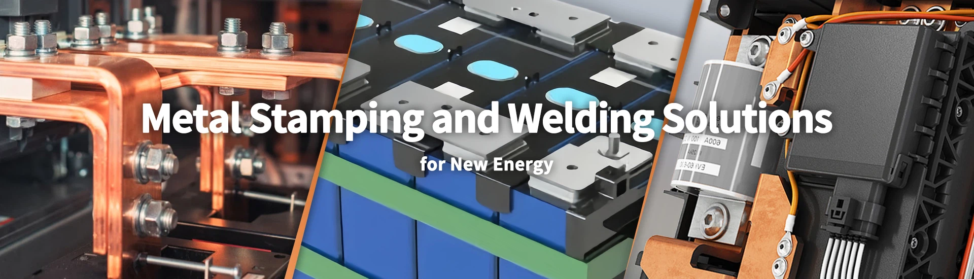
Custom Copper Stamping Part Manufacturer for Electrical and Industrial Components
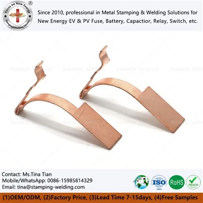
Xiamen Apollo manufactures custom copper stamping parts for electrical switches, relays, contactors, circuit breakers, and power distribution equipment. We process T2 copper, C11000 copper, and customer-specified copper materials through precision blanking, punching, bending, and progressive die stamping.
Copper Stamping Manufacturing Capabilities:
Materials: T2 copper, C11000 copper, and specified copper alloys.
Processes: Progressive die stamping, compound stamping, blanking, and precision bending.
Components: Electrical contacts, terminals, conductive plates and connecting parts.
Finishes: Bare copper, tin plating, nickel plating, and silver plating.
Production: Prototype development, tooling fabrication, and volume manufacturing.
Apollo supports drawing-based production from tooling assessment to finished-part inspection. Our engineering team reviews material thickness, bend geometry, burr direction, critical dimensions, and assembly interfaces before production. Inspection records and PPAP Level 3 documentation can be arranged according to customer project requirements.
Request a Factory Direct Quote
Explore Our Copper Stamping Parts Product Catalog
Browse precision copper terminals, electrical contacts, stamped connectors, and custom copper components for industrial applications.
-
![Customized Metal Stamping Copper]()
Customized Metal Stamping Copper
Add to Inquiry -
![Stamping Copper Sheet]() Add to Inquiry
-
![Electrical Contact Metal Copper Stamping Parts]()
Electrical Contact Metal Copper Stamping Parts
Add to Inquiry -
![Pressed Copper Stamping Sheet]() Add to Inquiry
-
![Progressive Die Stamped Copper Parts For MCCB]()
Progressive Die Stamped Copper Parts For MCCB
Add to Inquiry -
![Copper Stamped Pressing Cutting Assembly Parts]()
Copper Stamped Pressing Cutting Assembly Parts
Add to Inquiry -
![Bending Laser Cutting Stamping Copper]()
Bending Laser Cutting Stamping Copper
Add to Inquiry -
![Pressing Copper Stamping Bending Connecting Parts]()
Pressing Copper Stamping Bending Connecting Parts
Add to Inquiry -
![Copper Stamping Electrical Precision Part]()
Copper Stamping Electrical Precision Part
Add to Inquiry -
![Copper Stamping Electrical Parts]()
Copper Stamping Electrical Parts
Add to Inquiry -
![Copper Stamping Contact For Electrical Switch]()
Copper Stamping Contact For Electrical Switch
Add to Inquiry -
![China Copper Stamping Metal Parts]()
China Copper Stamping Metal Parts
Add to Inquiry



Material Standards, Tooling & Forming Processes
Copper stamping parts are selected according to the electrical, mechanical, and dimensional requirements of the finished component. High-conductivity copper grades are commonly used for current-carrying terminals and contacts, while copper alloys may be appropriate when a design requires a different balance of conductivity, strength, spring properties, or formability.
The material specification should identify the copper grade, temper, thickness, and applicable material standard. C11000 copper and T2 copper are examples of commonly specified copper materials, but they should not be treated as interchangeable without checking the governing standard and the customer's requirements. Conductivity depends on material composition and condition; where a minimum IACS value is required, it should be verified against the applicable material specification.
Progressive Die Stamping and Forming Control
For high-volume copper stamping parts, progressive die stamping can combine punching, notching, forming, and cut-off operations within a continuous production sequence. Compound dies, or single-operation tooling, may be more appropriate for simpler geometries, prototypes, or parts with particular dimensional constraints.
Tool design should account for the relationship between material thickness, punch-to-die clearance, edge quality and tool wear. The appropriate clearance depends on the copper grade, temper, thickness, and required cut-edge condition. Excessive clearance can increase rollover and burr formation, while insufficient clearance can raise cutting force and accelerate tool wear.
For formed electrical terminals and contacts, the manufacturing plan should also evaluate:
Burr height and orientation: Set acceptance criteria based on the mating interface, electrical clearance, and assembly direction.
Bend radius and springback: Account for material temper, grain direction where relevant, thickness and forming sequence.
Hole position and terminal profile: Identify functional datums and dimensions that affect assembly.
Flatness and contact area: Control the geometry of surfaces that must mate or carry current.
Progressive die stability: Monitor wear and dimensional drift across production runs.
Copper Stamping Parts Specifications
| Parameter | Specification basis | Verification method |
| Copper grade | T2, C11000 or customer-specified copper grade | Material certificate and grade verification |
| Material temper | As specified by the drawing and material standard | Material certificate or agreed test |
| Strip thickness | Drawing-defined nominal thickness and tolerance | Calibrated micrometer or thickness gauge |
| Electrical conductivity | Applicable material specification; IACS threshold defined by customer | Conductivity test when required |
| Critical dimensions | Drawing-defined tolerances; ±0.01 mm only where validated for the feature and process | Optical measurement, gauges, or CMM |
| Burr height | Maximum allowable height defined by drawing or control plan | Optical inspection or suitable burr measurement |
| Bend geometry | Defined angle, radius, and formed height | Profile measurement or dimensional inspection |
| Surface finish | Bare copper or specified plating system | Visual inspection and coating verification |
The table identifies the parameters to establish for a project. Actual values must be defined by the approved drawing, material standard, and inspection plan rather than applied as universal limits.
For parts requiring a specific material grade, see T2 Copper Stamping Parts.
Tooling Development and Design for Manufacturability
Before tooling manufacture, the DFM review should identify critical-to-quality dimensions, the datum scheme, material direction, burr direction, forming radii, and any features that could create excessive local strain. Where a component includes multiple bends or formed tabs, the forming sequence should be checked for interference and accumulated dimensional variation.
The first-article inspection should confirm that the tool produces the required geometry before release to volume production. For repeat orders, the control plan should define inspection frequency, tool maintenance criteria, and the response to out-of-tolerance measurements.
Advanced Joining, Insulation & Surface Treatments
Copper stamping parts frequently require secondary processing to achieve the finished assembly specification. Depending on the component design, these operations may include resistance welding, soldering, brazing, riveting, machining, or plating. Process selection should reflect the material combination, electrical path, mechanical load, and operating environment.
Joining Methods for Copper Components
Resistance welding is suitable for certain copper assemblies, but copper's high electrical and thermal conductivity affects heat generation and heat dissipation at the joint. Electrode design, applied force, current profile and weld duration therefore need to be established for the specific materials and joint geometry.
Soldering and brazing require compatible filler materials, controlled surface preparation and suitable thermal profiles. The process specification should define the required wetting, joint coverage and acceptance criteria. Where a connection carries current, visual inspection should be supplemented by electrical or mechanical testing when required by the product risk assessment.
Riveting may be suitable for joining copper contacts to supporting components when the joint design permits sufficient mechanical retention. If an in-die riveting operation is selected, the tooling must control component alignment, rivet deformation, and the resulting joint geometry.
Surface Plating and Corrosion Control
Bare copper, tin plating, nickel plating, and silver plating are selected according to the electrical interface and environmental conditions.
Bare copper offers high conductivity but may develop surface oxidation during storage or service. Plating can change contact behavior and corrosion performance, so coating selection must match the intended mating materials and operating conditions.
A plating specification should state:
Coating type and any required underlayer.
Minimum local thickness and measurement locations.
Permitted surface defects and coverage requirements.
Adhesion and corrosion tests where applicable.
Packaging and storage conditions intended to limit contamination or surface damage.
A coating thickness in the 3–10 µm range may be specified for some projects, but it is not a universal requirement for all copper stamping parts. The approved drawing and plating specification must define the applicable thickness and test method.
Electrical Performance and Assembly Validation
For current-carrying components, electrical performance depends on material conductivity, cross-sectional area, contact geometry, joint resistance, and the thermal conditions of the finished assembly. The component manufacturer should verify the characteristics specified in the drawing, while final temperature-rise qualification must account for the complete electrical assembly and its intended operating conditions.
Where the part is insulated or installed near adjacent conductive components, clearance, creepage distance, and dielectric performance should be evaluated at the assembly level according to the applicable design requirements.
Request Custom Technical Evaluation
Quality Control & Certifications at Apollo
Quality control for copper stamping parts should cover incoming material verification, tool setup, dimensional inspection, secondary processing, and final release. The inspection plan must distinguish functional dimensions from non-critical features so that measurement resources are concentrated on characteristics affecting assembly, electrical performance, and product safety.
Dimensional Inspection and Process Control
Depending on the part geometry and drawing requirements, dimensional inspection may use optical measuring equipment, calibrated gauges, profile measurement systems or CMM equipment. Critical characteristics should be measured against defined datums, with the method selected to suit the feature size, tolerance, and measurement uncertainty.
The control plan should address:
Material grade and thickness verification before stamping.
First-article approval after tooling setup or tool modification.
In-process checks for burrs, cracks, forming angle and critical dimensions.
Periodic monitoring of hole position, terminal height, and flatness.
Final inspection of quantity, surface condition, and packaging.
Lot identification and traceability for material and finished parts.
A stated dimensional tolerance, such as ±0.01 mm, must be confirmed for the particular feature and production process. It should not be applied indiscriminately to every dimension of a formed copper component.
Quality Documentation and Automotive Programs
Apollo's published product information references ISO 9001 and IATF 16949 in its manufacturing context. For a specific order, the applicable certification scope and validity should be confirmed before the credentials are used in a purchasing specification.
For automotive projects requiring PPAP Level 3, the submission package should be defined by the customer-specific requirements and agreed approval plan. Depending on the program, it may include:
Process flow diagram.
Process Failure Mode and Effects Analysis (PFMEA).
Control plan.
Material and performance test results.
Dimensional results for the production-representative sample.
Measurement system and process capability evidence where applicable.
CPK values should be reported only when the data set, sampling method, and calculation basis support the stated result. Documentation should correspond to the actual production process and approved part revision.
Production Consistency and Packaging
Copper stamping parts can be affected by tool wear, strip variation, handling damage and surface contamination. Production controls should establish inspection frequency, escalation rules, and traceability requirements for nonconforming batches.
Packaging must protect thin stamped parts from bending, scratches, moisture, and deformation during shipment. For plated contacts, packaging should also limit surface contamination and avoid materials that may damage the specified finish.
Frequently Asked Questions
Q: 1. Which copper grade should be specified for electrical stamping parts?
A: T2 copper and C11000 copper are common options for conductive components, but selection depends on the governing material standard, conductivity requirement, temper, and forming geometry. The drawing should specify the grade and acceptance criteria. Where conductivity is critical, verify the required IACS value against the applicable material specification.
Q: 2. Can copper stamping parts achieve a tolerance of ±0.01 mm?
A: A ±0.01 mm tolerance may be feasible for selected features, depending on material thickness, tool design, feature geometry and measurement method. It should not be assumed for every stamped or formed dimension. Define critical datums and tolerances on the drawing, then confirm capability through tooling trials and first-article inspection.
Q: 3. How can burrs and springback be controlled in copper stamping?
A: Burr formation depends on punch-to-die clearance, tool condition, material temper, and cutting geometry. Springback also varies with material properties, thickness, and bend radius. Appropriate tooling design, controlled forming sequences, regular die maintenance, and dimensional inspection help maintain repeatability across production lots.
Q: 4. What surface treatment is appropriate for copper electrical contacts?
A: Bare copper, tin, nickel, or silver plating may be suitable depending on the mating material, contact pressure, corrosion exposure, and operating conditions. The specification should identify coating type, minimum thickness, coverage, and required tests. Contact resistance and environmental performance should be validated for the intended assembly rather than inferred from plating thickness alone.
Request a Custom Copper Stamping Parts Quote
For a drawing-based copper stamping project, provide the material grade, strip thickness, critical dimensions, annual volume, and required surface treatment. These details allow the manufacturing team to assess tooling design, forming sequence, inspection requirements, and the proposed production route.
Upload your 2D drawings in .DWG or PDF format, 3D models in STEP format, or a technical specification identifying critical-to-quality characteristics. Include any requirements for conductivity, burr height, bend geometry, plating thickness, joint strength, or PPAP documentation.
Apollo can review the available information for DFM considerations and quotation preparation. A preliminary response within 24 hours may be targeted for complete inquiries, subject to drawing complexity and technical review requirements.
We're well-known as one of the leading copper stamping part manufacturers and suppliers in China. Please feel free to buy high quality copper stamping part at competitive price from our factory. For more information, contact us now.
