Detailed explanation of Electrical copper stamping parts processing technology
Mar 23, 2026
Material selection
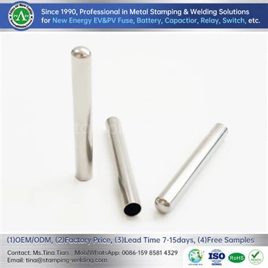
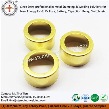
The material selection for the processing of Electrical copper stamping parts should take into account conductivity, formability, and cost, with the core divided into two levels: material category and grade. Divided by chemical composition, pure copper and brass are commonly used in stamping processing: pure copper (purple copper) has outstanding conductivity and thermal conductivity, and is suitable for high-precision electronic components, electrical connection parts, and other scenarios that require high conductivity efficiency; Brass has better strength and wear resistance, making it suitable for structural components that can withstand mechanical loads and wear.
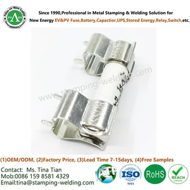
The commonly used copper grades for Copper stamping contact for electrical switches in China include T1, T2, T3, etc. The higher the grade, the higher the copper purity, and the better the conductivity and formability. In production, it is necessary to accurately match the grade according to product functional requirements to avoid excessive performance or cost waste.

Core process flow
The complete process flow of Electrical copper stamping parts covers three stages: raw material pretreatment, forming processing, and post-processing, with each link closely connected to ensure the quality of the finished product.
Firstly, in the cutting process, the copper raw materials are processed into billets that meet the size requirements through cutting, punching, or laser cutting according to the product drawings, laying the foundation for subsequent forming.
Subsequently, surface pretreatment is carried out to remove surface oxide layers and impurities through acid washing, alkali washing, or electrolytic polishing, improving the stamping performance of the material and avoiding defects such as cracking and burrs. The stamping forming of Stamping copper sheet is the core process, which requires the completion of mold design and preheating.
Then, the stamping speed and pressure are determined based on the material thickness and structural complexity, combined with mold lubrication to reduce wear.
Finally, the target shape is achieved through processes such as punching, bending, and stretching. After forming, the finished product is inspected, cleaned, and packaged in sequence to ensure that the size and performance meet the standards and the surface is clean, providing assurance for transportation and use.

Mold and Equipment
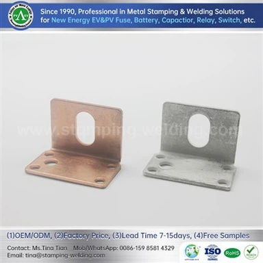
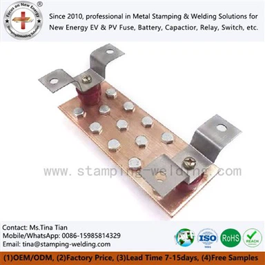
Stamping molds and equipment are key factors determining the precision and production efficiency of Custom copper stamping. Mold design should revolve around the shape, size, and forming requirements of the product. Mold materials often include wear-resistant and high-strength materials such as high manganese steel and Cr12MoV. The structure includes convex molds, concave molds, guide columns, guide sleeves, and other components. It is necessary to ensure accurate matching with the size of the billet while also considering the feasibility of forming complex structures. In terms of equipment selection, it is necessary to match the type of press according to the accuracy of the Metal stamping part and batch requirements. At the same time, by preheating the mold and accurately controlling the stamping parameters, the service life of the mold can be extended, and the consistency and stability of batch production can be improved.
Quality control
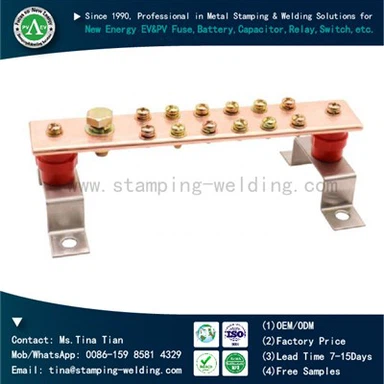
The quality control of Copper sheet metal fabrication runs through the entire processing process, forming a closed-loop control from raw materials to finished products. During the raw material stage, it is necessary to verify the purple bronze plate number and purity to ensure that the basic performance meets the standards; During the stamping process, by monitoring the mold temperature, stamping parameters, etc., the process can be adjusted in a timely manner to avoid defects such as deformation, cracking, burrs, etc; The focus of the finished product inspection process is to verify the dimensional accuracy (controlled within ± 0.05- ± 0.1mm, with high-precision parts up to ± 0.01mm), surface quality, and mechanical properties to ensure compliance with drawings and industry standards. The cleaning and packaging processes are professionally treated to avoid surface contamination and transportation damage, ultimately delivering high-quality Copper stamping parts that meet customer needs.
contact us
We are committed to providing stable and reliable Electrical copper stamping parts processing solutions for fields such as electronics, electrical engineering, and mechanical engineering. We can provide customized process planning and mass production support based on product drawings and application conditions. Customers with detailed processing parameters or mass production needs are welcome to consult, and we will quickly provide professional process advice and delivery solutions.