Detailed professional knowledge of ceramic metallization industry
Jun 03, 2026
product definition
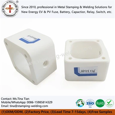
Ceramic metallization is a special surface treatment technology that forms a dense metal film on the surface of a ceramic substrate to make the ceramic weldable and conductive, thereby achieving a reliable connection between ceramics and metal materials. The essence of this technology is to build a transitional intermediate layer on the surface of ceramics that is chemically stable and difficult to wet by solder. This intermediate layer can not only react chemically with the ceramic matrix to form a strong bond, but also form good wetting and diffusion with metal solder, thereby achieving airtight sealing or electrical interconnection between dissimilar materials. In the field of power semiconductor packaging, Metallized Ceramic Housing for Power Semiconductors is a key component of IGBT modules, MOSFET packaging and thyristor housings. These products use a metallization process to form a solderable metal layer in specific areas of the ceramic housing for solder assembly with copper substrates, lead frames or terminals, while the ceramic body provides electrical insulation and high thermal conductivity channels. Metallized Ceramic Insulating Tubes Metallizing Ceramic Part refers to metallized ceramic insulating tubes and metallized ceramic parts, which are widely used in high-voltage relays, vacuum interrupters, electric vacuum devices, X-ray tubes and other fields.
The metallized layer is usually located on the end face of the ceramic tube or in specific areas on the inner and outer surfaces and is used for welding and sealing with metal flanges or electrode leads. Metallized Ceramics for Electrical Components is a general term for metallized ceramics for electrical components, covering a variety of application scenarios from high-voltage contactors to low-voltage electrical switches. High-Strength Metallized Ceramic Components are high-strength metallized ceramic components that emphasize the bonding strength between the metallized layer and the ceramic matrix, usually using the molybdenum-manganese method or active metal brazing method to enable the metallized layer to withstand tensile or shear loads without peeling off. HVDC contactor ceramic enclosure is a high-voltage DC contactor ceramic cavity. It is a typical application of metallized ceramics in the field of new energy high-voltage DC protection. Its metallized layer is used for reliable connection with the metal contact system and sealing cover. At the same time, the interior of the ceramic cavity needs to withstand long-term burning of DC arcs. Precision Metallized Ceramics, or precision metallized ceramics, represent the industry's higher standards for dimensional tolerance, metallized layer position accuracy and surface quality. They are usually used in aerospace, medical equipment and high-end industrial control fields.

Manufacturing process
The manufacturing process of ceramic metallization is a technical system involving multiple precision control links. The following description takes the molybdenum-manganese metallization of alumina ceramics as a typical process flow. Step 1: Preparation of ceramic matrix – Mix alumina powder with additives such as binders, plasticizers, and dispersants to form a slurry, and obtain a green body of the desired shape through tape casting, dry pressing, or isostatic pressing. Tape casting is suitable for the production of large-sized thin ceramic substrates, dry pressing is suitable for small and medium-sized thick-walled parts, and isostatic pressing is suitable for tubular or special-shaped ceramic parts. The green body is dried and degummed (slowly heated to 400-600°C to remove organic matter), and then sintered in a high-temperature furnace (alumina ceramics are about 1600-1700°C) to obtain a dense ceramic matrix. The sintered ceramic matrix needs to be surface ground or peripherally processed to meet dimensional tolerance requirements.
Step 2: Preparation of metallized slurry – Weigh molybdenum powder, manganese powder and additives (such as silica, aluminum oxide, magnesium oxide and other fluxes) according to the formula, mix them, add organic carriers (terpineol, ethyl cellulose, etc.) and grind to make a paste slurry with appropriate viscosity. The solid content, particle size and rheological properties of the slurry directly affect the thickness, density and sintering shrinkage of the metallization layer. Step 3: Metallization layer coating – Apply the metallization slurry to the predetermined area of the ceramic substrate using screen printing, spraying, dipping or brushing. For Metallized Ceramic Housing for Power Semiconductors, screen printing is often used to achieve precise control over the shape and position of the metallized areas. For Metallized Ceramic Insulating Tubes Metallizing Ceramic Parts, the metallization of the inner or outer walls of tubular parts usually uses dip coating or spraying processes, combined with special protective tooling. The coated parts need to be dried in an oven (about 100-150°C) to volatilize the organic carrier.
Step 4: Primary metallization sintering – Place the coated and dried ceramic parts in a hydrogen-protective atmosphere furnace for high-temperature sintering. The sintering temperature is usually between 1300-1500℃ (depending on the formula), and the holding time is about 30-60 minutes. During the sintering process, the molybdenum-manganese powder undergoes sintering densification, and at the same time, the glass phase migrates from the molybdenum-manganese layer to the ceramic interface and reacts with the alumina in the ceramic to form a transition intermediate phase. The function of a hydrogen atmosphere is to reduce the oxide film on the surface of metal powder and promote sintering activity. After sintering, the metallization layer forms a strong chemical bond with the ceramic matrix. Step 5: Nickel plating. Electroless nickel plating or electroplating nickel is performed on the surface of the molybdenum manganese layer after primary metallization and sintering. Nickel plating has two purposes: one is to protect the molybdenum-manganese layer from oxidation, and the other is to provide a solderable surface (the wettability of solder to nickel is better than that of the molybdenum-manganese layer). The thickness of the nickel plating layer is usually controlled at 2-8 microns. If it is too thin, the coating may be dissolved by the solder during welding. If it is too thick, it may be caused by internal stress.

Detailed display
The quality of ceramic metallized products is often reflected in microscopic details that can be observed with the naked eye or perceived through simple tests. The first is the continuity and adhesion strength of the metallization layer - place the Metallized Ceramic Housing for Power Semiconductors under good light and observe it. A high-quality metallization layer should have a uniform metallic luster, clear and sharp edges, and no visible peeling or other defects. Use 3M tape to stick it on the surface of the metallized layer and peel it off quickly. There should be no metal particles stuck. The second is the positioning accuracy of the metallized area. For tubular parts such as Metallized Ceramic Insulating Tubes Metalizing Ceramic Part, the width uniformity and concentricity of the end-face metalized ring directly determine the sealing reliability when welding to the metal flange. Excessive deviation may lead to local failure to weld or solder overflow. The third detail is the quality of the nickel plating layer - a qualified nickel plating layer should be in a uniform matte or semi-bright state, with no obvious color difference, pinholes or blisters. For the HVDC contactor ceramic enclosure, immerse the nickel-plated ceramic cavity in standard flux.
After taking it out, observe that the metallized surface should be completely covered by flux and there is no solder-rejection area, which directly reflects the solderability of subsequent soldering. The fourth detail is the state of the ceramic matrix after sintering - metallization and sintering undergo high-temperature cycles above 1300°C, and the unstable quality of the ceramic matrix may cause micro-cracks or warping. Place Precision Metallized Ceramics flat on a marble platform and use a feeler gauge to check the flatness; for tubular parts, check the parallelism of both end faces. The last detail that is easily overlooked is the cross-sectional structure of the metallization layer - observe the cross-section of the metallization layer through a metallographic microscope. The metallization layer of a high-quality product should be dense and without through-holes, and the interface with the ceramic substrate should present a canine-tooth interlocking shape rather than a straight gap. Our company conducts item-by-item inspections of the above details for each batch of ceramic metallized products and keeps metallographic photos and solderability test records to ensure that every product delivered meets engineering-level quality requirements.

Application industry
The application industries of ceramic metallization products cover a wide range of fields from power electronics to new energy, from aerospace to medical devices. In the power semiconductor industry, Metallized Ceramic Housing for Power Semiconductors is a core component of IGBT modules, MOSFET and diode packaging. IGBT modules are widely used in frequency converters, electric welding machines, induction heating and rail transit traction systems. Their ceramic shells need to meet the comprehensive requirements of high-voltage insulation (typical value 1200V-6500V), high thermal conductivity and heat dissipation, and long-term thermal cycle reliability. In the field of power transmission and distribution, HVDC contactor ceramic enclosure is used in electric vehicle charging facilities, photovoltaic energy storage systems and DC distribution cabinets. High-voltage DC contactors need to reliably break fault current under DC conditions. The metallization quality of the ceramic cavity directly determines the air tightness and arc extinguishing performance of the contactor. In the field of electric vacuum devices, Metalized Ceramic Insulating Tubes Metalizating Ceramic Part is used in vacuum arc extinguishers (core components of medium and high voltage circuit breakers), traveling wave tubes, magnetrons and X-ray tubes.
Metalized ceramic parts need to maintain long-term airtightness in high vacuum environments. The porosity of the metallized layer and the welding airtightness are key quality indicators. In the aerospace and military fields, High-Strength Metallized Ceramic Components are used in missile seeker casings, satellite transponder substrates and aero-engine sensor packaging. There are extremely high requirements for the materials' high temperature resistance, impact resistance and long-term reliability. In the fields of industrial control and general electrical, Metallized Ceramics for Electrical Components covers low-voltage electrical appliances (such as contactors, relays, thermostats), high-voltage switches, gas discharge lamp starters and spark plugs. In the field of medical equipment, Precision Metallized Ceramics is used in feed-through connectors for implantable medical devices (such as pacemakers, neurostimulators), CT detectors and laser surgical instruments, which require the metallization layer to be biocompatible and able to pass strict sterilization tests.

contact us
We provide Alumina Metallized Ceramics one-stop service from ceramic molding, precision grinding, molybdenum manganese method/AMB metallization, nickel plating to welding assembly. The engineering team can quickly complete the process plan design according to your voltage level, air tightness requirements and welding interface parameters. Welcome to submit drawings or technical specifications for process evaluation and sample docking.