Analysis Of Bare Copper Busbar Laser Cutting Technology: Principles, Advantages, And Process Optimization
Apr 04, 2025
Key applications and processing challenges of bare copper busbars
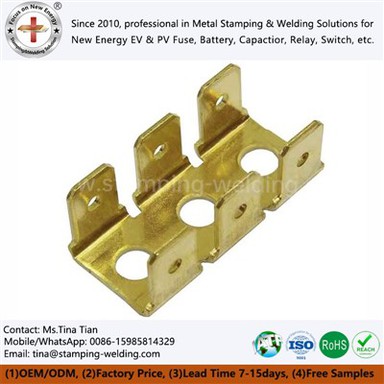
As the core conductive material in the power system, bare copper busbars are widely used in power transmission and transformation equipment, high and low voltage electrical appliances, and motor windings. Its performance requirements include not only excellent conductivity and mechanical strength, but also strict standards for processing accuracy and surface quality. Traditional processing techniques such as punching and drawing have problems such as burr residue, stress concentration and long processing cycle, which are difficult to meet the precision requirements of high-end equipment for conductive parts. Laser cutting technology, with its non-contact processing characteristics, provides an innovative solution for the high-precision processing of bare copper busbars.

Core principles and process characteristics of laser cutting technology
(I) Technical principle
Laser cutting focuses a high-power density laser beam (energy density can reach more than 10⁶ W/cm²) to instantly heat the surface material of the Copper BusBar to the vaporization temperature (about 2567℃) to form tiny vaporization holes. At the same time, high-pressure auxiliary gas (such as nitrogen or oxygen) coaxial with the beam blows away the molten metal residue, and continuous cutting is achieved as the laser head moves along the preset trajectory. This process combines heat conduction, vaporization phase change, and airflow dynamics to achieve millimeter-level to micron-level precision processing.
(II) Process characteristics
Stress-free processing: Non-mechanical contact cutting avoids the residual mechanical stress of traditional punching and shearing processes, ensures the stability of the internal organizational structure of the Electrical Bus Bar, and is particularly suitable for the connection requirements of precision electrical components.
Ultra-precision edge quality: The cutting edge roughness can reach Ra≤12.5μm, without burrs, peeling and other defects, reducing subsequent grinding processes, and directly meeting the insulation packaging requirements.
Complex shape adaptability: Supports arbitrary two-dimensional and three-dimensional trajectory cutting, and can process ultra-thin row materials and special-shaped structures with a width-to-thickness ratio of >10, breaking through the shape limitations of traditional mold processing.

Technical optimization plan for copper material characteristics
(I) Countermeasures for high-reflective material processing
Copper has the characteristics of high reflectivity (absorption rate of 1μm wavelength laser <5%) and high thermal conductivity (401 W/(m・K)), which easily leads to laser energy attenuation and thermal deformation. Stable cutting is achieved through the following technical improvements:
Anti-high-reflective optical path design: adopt a fully enclosed optical path system and multi-layer dielectric film lenses to reduce the damage of reflected light to optical components and ensure the stability of energy output.
Energy modulation technology: combining pulsed laser and waveform optimization algorithm, through peak power increase (>10 kW) and pulse width control (10-100μs), quickly breaks through the material reflection threshold and achieves efficient vaporization.
(II) Coordinated control of process parameters
Cutting speed matching: dynamically adjust the speed (0.5-5m/min) according to the thickness of the plate (0.5-30mm) to avoid slag residue caused by too fast speed or thermal deformation caused by too slow speed.
Gas pressure optimization: 0.5- 2MPa high-pressure auxiliary gas is used to ensure timely discharge of slag and inhibit oxidation reaction (the thickness of the oxide layer is less than 10μm when nitrogen protection is used).
Comparison of industry advantages of laser cutting technology
| Performance indicators | Laser cutting | Traditional punching and shearing | Electro-spark machining |
| Dimensional accuracy | ±0.1mm | ±0.5mm | ±0.05mm |
| Surface roughness | Ra≤12.5μm | Ra≥25μm | Ra≤6.3μm |
| Material utilization rate | >95% | 70%-85% | 85%-90% |
| Processing efficiency | 50-200 pieces/hour | 10-30 pieces/hour | 20-50 pieces/hour |
| Adaptability to complex shapes | Excellent | Poor | Good |
Compared with traditional processes, laser cutting technology reduces mold costs and shortens the proofing cycle (from 72 hours to 4 hours) through moldless production, while reducing auxiliary processes such as annealing and grinding, and reducing the overall production cost by 30%-50%. In emerging fields such as 5G base stations and new energy vehicles, its efficient and flexible processing capabilities significantly improve the integrated design space of conductive components.
Quality control and future development trends
(I) Key points of process control
Environmental parameter monitoring: Maintain the processing environment temperature (20±2℃) and humidity (≤60% RH) to prevent copper surface oxidation from affecting cutting quality.
Online detection integration: Real-time monitoring of cutting trajectory deviation (accuracy ±0.05mm) through a CCD visual system, combined with an AI algorithm to automatically compensate for motion error.
(II) Technology evolution direction
Ultrafast laser application: Femtosecond (10⁻¹⁵ second level) laser technology can achieve "cold processing", significantly reduce the heat affected zone (<50μm), and improve the processing reliability of ultra-thin busbars (<0.1mm).
Intelligent production line: Based on digital twin technology, self-optimization of cutting parameters and predictive maintenance of equipment status are realized, and processing efficiency is improved by more than 20%.

Conclusion
Laser cutting technology has become the mainstream choice for bare copper busbar processing due to its precision, flexibility, and efficiency. With the continuous breakthroughs in high-power fiber lasers and intelligent control algorithms, this technology will continue to be applied in new energy, high-end equipment manufacturing and other fields, and promote the processing of conductive materials towards high precision and greenness. Industry participants need to continuously optimize process parameters and strengthen equipment integration innovation to cope with the ever-increasing market demand.
contact us