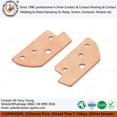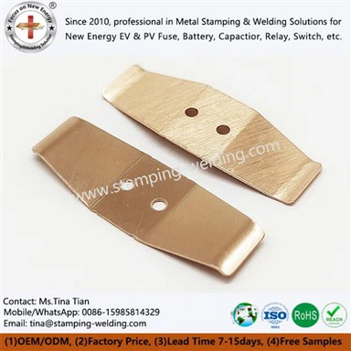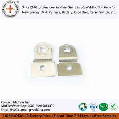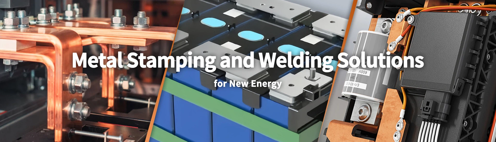


Copper Stamping Parts
Copper Stamping Parts are precision-formed components produced from copper sheet or strip for electrical applications. Key controls cover hole position, bending geometry, burrs, material grade, thickness, and conductivity. Our OEM production integrates stamping, tooling, plating, machining, and testing for rapid sampling and stable batch production, supported by ISO 9001 and IATF 16949 systems.
- Fast Delievery
- Quality Assurance
- 24/7 Customer Service
Product Introduction
Copper Stamping Parts are precision-formed components made from copper sheet or strip through punching, blanking, bending, and progressive die stamping. They provide controlled geometry, electrical conductivity, and dimensional consistency for terminals, contacts, fuse components, switches, relays, connectors, EV, PV, and ESS applications. Custom material grades, thicknesses, geometries, and surface treatments are available.

Key features of Copper Stamping Parts
Precision Stamping
Utilizes copper sheets or strips for precision stamping-incorporating punching, blanking, bending, and progressive die forming-to achieve complex geometries and consistent dimensional control.
High-Conductivity Copper
Employs high-purity copper materials that balance excellent electrical conductivity with superior formability, making them ideal for components such as fuses, terminals, switches, and relays for Copper Stamped Components.
Custom Electrical Components
Offers customization of dimensions, hole patterns, bending, material thickness, and surface finishes; copper stamped parts can be developed from technical drawings to meet mass-production requirements for EV, PV, and ESS applications.

Quality Control of Copper Stamping Parts
Dimensional & Forming Control
Key inspections focus on hole locations, external dimensions, bending angles, and forming heights. Stamping deformation and dimensional deviations are strictly controlled to ensure consistency during mass assembly.
Edge & Surface Inspection
Inspections target common defects such as burrs, cracks, scratches, and deformation. The condition of stamped edges is controlled to meet assembly requirements for terminals, contacts, and connectors.
Material & Electrical Inspection
Material grade, thickness, and electrical conductivity are verified against product specifications. Combined with surface finish inspections, this ensures the copper stamped parts meet requirements for electrical connectivity and long-term durability.

Frequently Asked Questions about Copper Stamping Parts
Q:1. What copper materials are suitable for Copper Stamping Parts?
A: High-purity copper is commonly selected when electrical conductivity is the primary requirement. Material grade and thickness can be specified according to the component design, stamping process, forming requirements, and electrical performance required for fuses, terminals, switches, relays, and connectors.
Q:2. How is dimensional accuracy controlled during copper stamping?
A: Critical dimensions such as hole locations, overall size, bending angles, and forming heights are checked against technical drawings. Precision tooling and controlled stamping parameters help reduce deformation and dimensional variation, supporting consistent fit and assembly across mass-produced Copper Stamping Parts.
Q:3. How are burrs and other edge defects controlled?
A: Stamped copper parts are inspected for burrs, cracks, scratches, and deformation after forming. Particular attention is given to cutting and punching edges, since excessive burrs can affect assembly, electrical contact, or component handling. Additional deburring can be applied when required by the drawing.
Q:4. Can Copper Sheet Stamping be customized for electrical applications?
A: Yes. Copper Stamping Parts can be produced according to specified dimensions, hole patterns, bending geometry, material thickness, and surface finish. This allows the component design to match the electrical and mechanical requirements of fuses, terminals, switches, relays, connectors, and other electrical assemblies.
Q:5. How is the electrical performance of copper stamped parts verified?
A: Material grade, thickness, and electrical conductivity are verified against the approved product specifications. Where required, surface finish and contact areas are also inspected to ensure the finished copper component provides the required electrical connection and remains suitable for its intended operating environment.
Q:6. What inspections are important for mass-produced copper stamped components?
A: For mass production, inspection typically covers dimensional accuracy, forming geometry, burrs, surface condition, material specifications, and electrical properties. Controlling these characteristics throughout production helps maintain batch-to-batch consistency and reduces assembly problems in downstream electrical equipment.

Contact Us
Send your 2D/3D drawings, copper material specification and annual volume for DFM review, tooling evaluation and a factory quotation.

Hot Tags: Copper Stamping Parts,Copper Stamping Manufacturer,Custom Copper Stamping,Copper Sheet Stamping,Copper Strip Stamping,Precision Copper Stamping,Progressive Die Stamping,Copper Stamped Components,OEM Copper Stamping Parts,Custom Copper Stamping Parts,Copper Electrical Components,Copper Fuse Components,Copper Terminal Stamping,EV Copper Stamping Parts,Copper Stamping Factory China