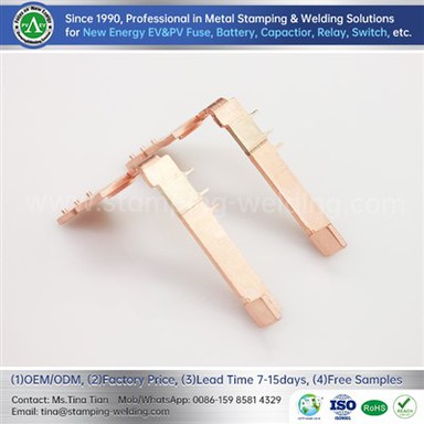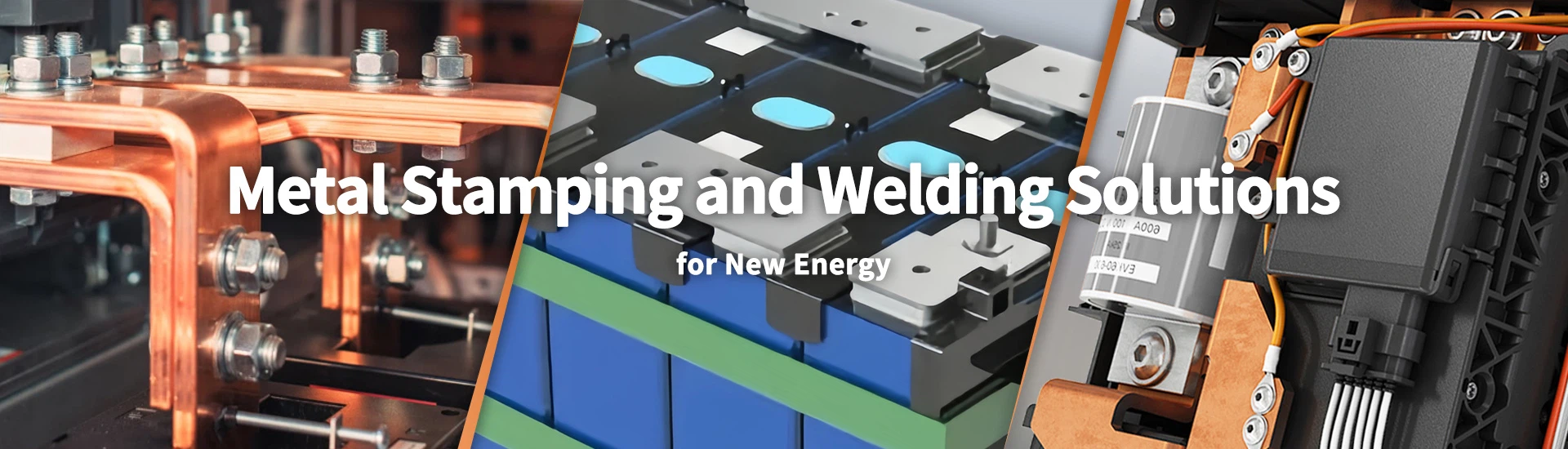


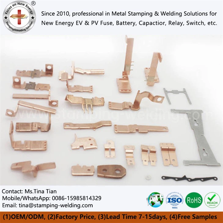
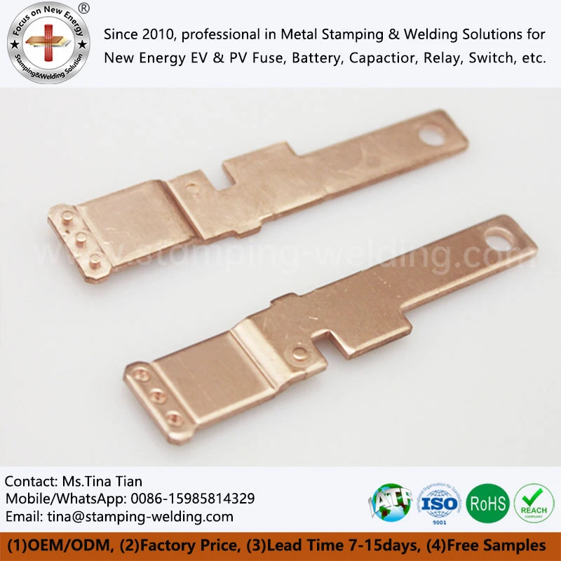
Precision Copper Stampings
Precision Copper Stampings are made for electrical and mechanical connection components requiring accurate forming and stable material properties. Progressive Die Stamping & Precision Forming delivers repeatable copper components, while Technical Specifications and Quality Assurance & Production Control verify material, dimensions, surface and functional requirements. Factory-direct production offers free samples in 1–2 days, new-tool samples in 20–30 days, and bulk orders in 15–20 days after confirmation and payment.
- Fast Delievery
- Quality Assurance
- 24/7 Customer Service
Product Introduction
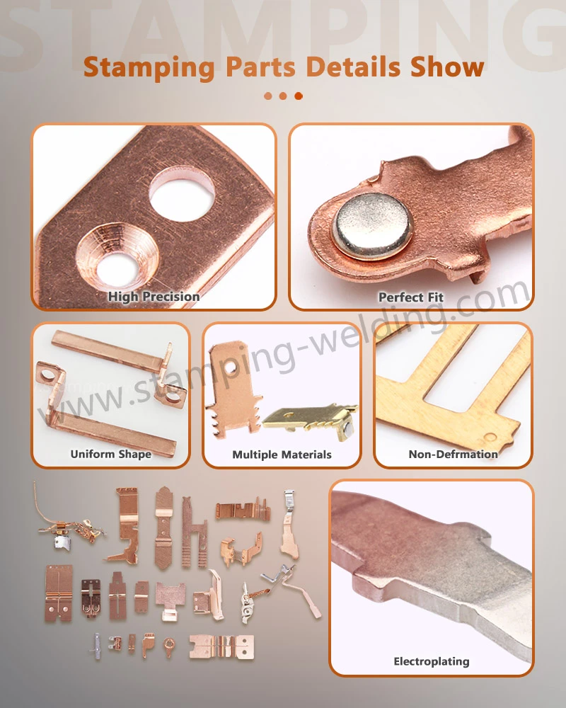
Electrical components require accurate contact geometry, stable assembly dimensions and controlled conductive paths. Precision Copper Stampings are produced from copper and copper-alloy sheet or strip through progressive die stamping, punching, bending and forming. Typical products include relay copper sheets, connector terminals, switch components, MCCB contact parts and other electrical copper stamped components. The material can be selected according to conductivity, hardness and forming requirements, while silver or tin plating can be specified for designated contact areas.
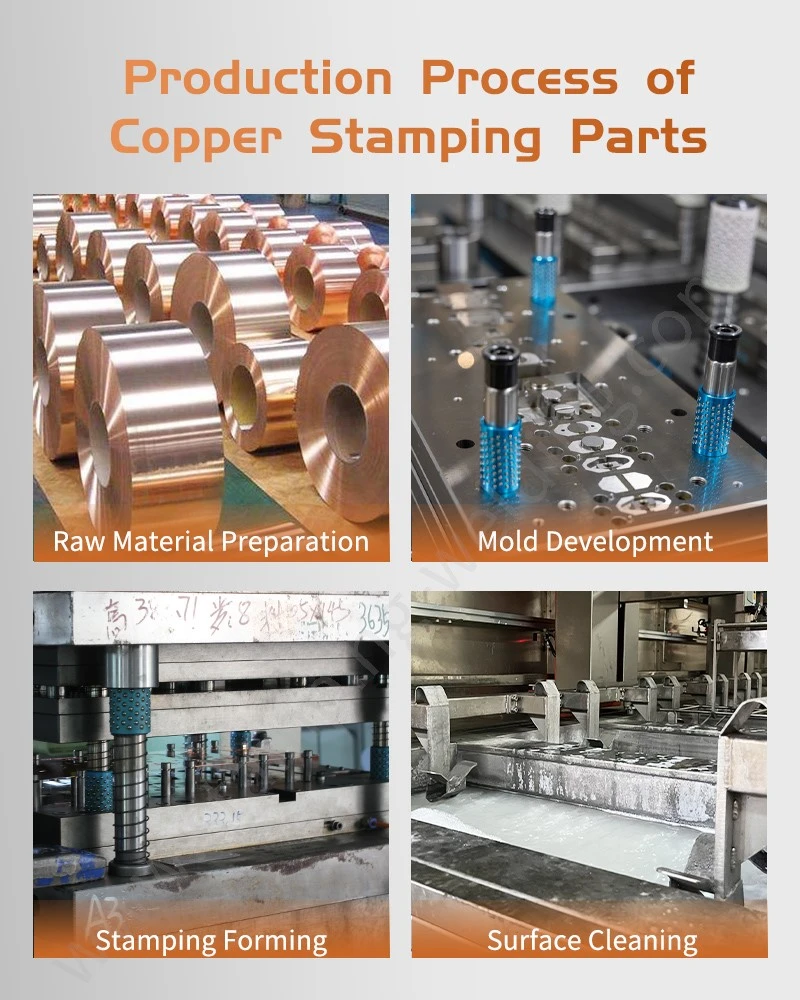
Manufacturing process of Precision Copper Stampings
Progressive Die Stamping
Multiple die stations perform blanking, punching, bending and forming in a controlled Precision Copper Stamped Parts production sequence. This reduces intermediate handling and supports repeatable production of copper stamped components.
Precision Punching & Bending
Punching, bending and forming operations establish the required terminal profile, mounting geometry and contact position. Tool clearance and forming conditions are adjusted according to copper grade and sheet thickness.
Burr & Edge Control
Cutting conditions and die clearance are controlled to reduce excessive burrs on electrical contact and assembly surfaces. Secondary deburring or edge treatment can be added when required for Copper Stamping Electrical Precision Parts.
Plating & Secondary Processing
Silver or tin plating can be applied to specified contact areas. Additional flattening, forming, welding or assembly operations can be incorporated when required by the component design for Copper Stamped Pressing Cutting Assembly Parts.
Technical Specifications of Precision Copper Stampings
| Product Type | Precision Copper Stampings |
|---|---|
| Base Material | Pure Copper / Copper Alloy |
| Material Form | Copper Sheet / Copper Strip |
| Stamping Method | Progressive Die Stamping |
| Operations | Blanking, Punching, Bending, Forming |
| Electrical Function | Conductive Contact / Terminal / Connector |
| Dimensional Tolerance | According to Customer Drawing |
| Burr Control | Controlled on Critical Contact Edges |
| Surface Treatment | Silver Plating / Tin Plating / As Specified |
| Contact Surface | Plated or Unplated According to Application |
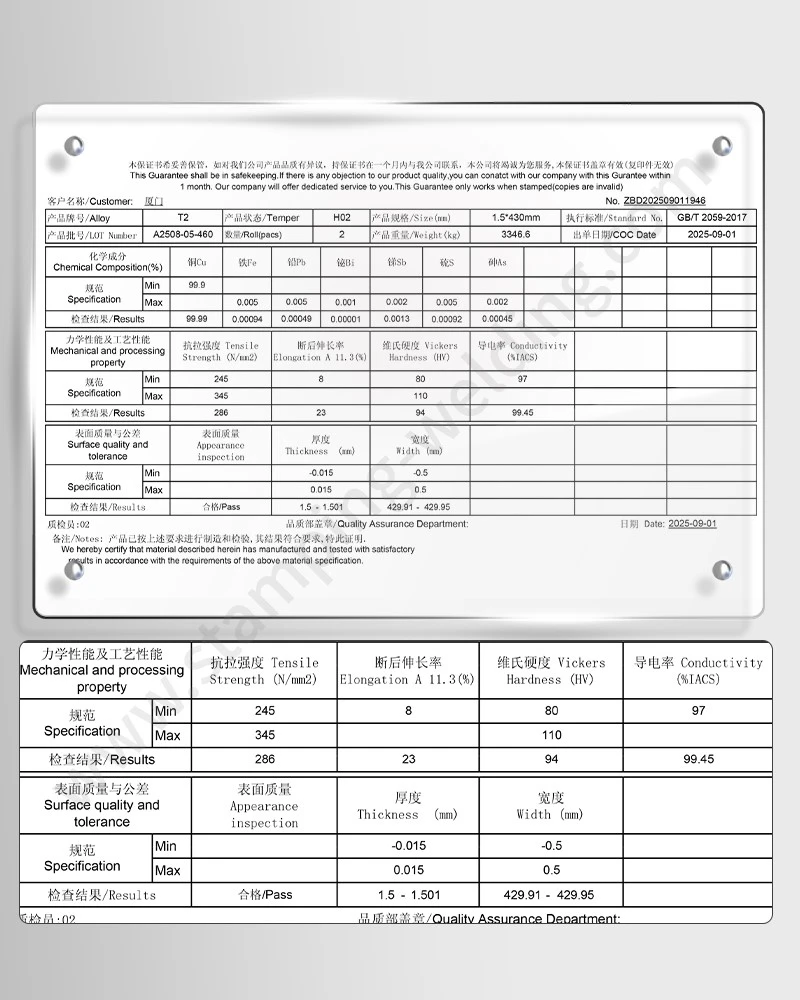
Quality Assurance of Precision Copper Stampings
Process Parameter Control
Press stroke, feeding accuracy, die clearance and forming conditions are monitored during copper stamping to maintain stable part geometry throughout production.
Dimensional & Surface Inspection
Critical dimensions, hole positions, bend angles, edge conditions and surface appearance are checked according to drawing requirements and inspection procedures for Progressive Die Stamped Copper Parts for MCCB.
Electrical & Functional Verification
Where specified, contact resistance, assembly fit, plating condition and functional characteristics are verified before batch release. Inspection records can support customer quality documentation and traceability requirements for Pressed Copper Stamping Sheet.
Frequently Asked Questions about Precision Copper Stampings
Q:1. How does progressive die stamping improve the production of precision copper stamped parts?
A: Progressive die stamping combines blanking, punching, bending and forming within sequential die stations. This reduces intermediate handling and keeps critical features in one production flow, supporting consistent hole positions, bend geometry and contact profiles for high-volume copper stamping production.
Q:2. What copper materials can be used for precision stamped components?
A: Pure copper and copper alloys can be selected according to conductivity, hardness, thickness and forming requirements. The material specification is confirmed before tooling and production, allowing the stamped part to meet the required electrical function, mechanical strength and dimensional requirements.
Q:3. What dimensional requirements can be controlled on copper stamping parts?
A: Dimensional control can cover overall dimensions, hole positions, bend angles, contact profiles and other drawing-defined features. Inspection methods are selected according to the part structure, while stamping and forming conditions are monitored to maintain repeatable geometry across production batches.
Q:4. How are burrs controlled on precision copper stamped parts?
A: Burr formation is controlled through die clearance, tool condition and stamping parameters matched to the copper material and thickness. Critical contact or assembly edges receive closer inspection, with secondary deburring or edge treatment available when required by the component specification.
Q:5. Can precision copper stampings include silver or tin plating?
A: Yes. Silver or tin plating can be specified for designated contact surfaces according to the electrical and environmental requirements of the component. Plating coverage and thickness are defined by the customer specification, with surface inspection performed before batch release.
Q:6. What inspections are performed on precision copper stamped components?
A: Quality control can include dimensional inspection, visual inspection, burr evaluation, plating inspection and assembly-related checks. Inspection requirements are established from the product drawing and technical specification, with production records used to monitor consistency across copper stamping batches.
Contact Us
Send your 2D/3D CAD drawings, material grade, copper thickness and annual volume for an engineering review.
We can assess stamping feasibility, forming sequence, tooling requirements, plating options and production method before quotation.
Hot Tags: Precision Copper Stampings,Copper Stamping Parts,Precision Copper Stamping,Copper Strip Stamping,Custom Copper Stamping,Copper Stamping Manufacturer,Copper Stamping Supplier,Progressive Die Stamping,Precision Punching and Bending,Precision Copper Stamped Parts,Electrical Copper Stamping Parts,OEM Copper Stamping,Silver and Tin Plating,Electrical Connection Parts