Technological Innovation Of Copper Stamping Drives The Upgrading Of Electrical Components
Apr 18, 2025
Copper stamping, as a key component of core electrical components such as relays, switches, and contactors, has become an important breakthrough for industry technological upgrading in recent years, thanks to its unique material properties and process advantages. In 2025, with the application of new materials, the optimization of processing techniques, and the growth of market demand, the Stamping Copper Sheet industry is embracing a new round of development opportunities.

Material Properties Establish Core Advantages
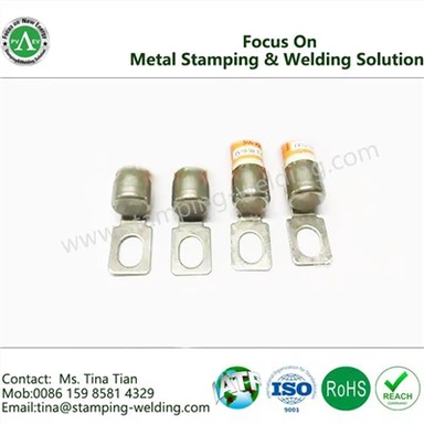
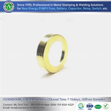
Copper (with a pure copper content of ≥99.95%, also known as red copper) has become the preferred material for stamping parts of electrical components due to its excellent electrical conductivity (second only to silver), thermal conductivity, and corrosion resistance. Compared with traditional materials such as phosphor bronze, copper stamping performs better in terms of resistivity and thermal stability, which can significantly reduce the energy loss and temperature rise during the operation of electrical components. In addition, the high plasticity of copper enables it to be processed into complex shapes through the stamping process, meeting the micron-level tolerance requirements of components such as precision contacts and shrapnel in relays and contactors.
Industry data shows that stamping parts made of high-purity copper can increase the service life of electrical components by 10%-15% and reduce the contact resistance by more than 30%, contributing to the high-efficiency development of fields such as new energy vehicles and smart home appliances.

Process Innovation Drives Efficiency Improvement
Aiming at the characteristic of copper being soft and prone to sticking to materials, new mold steels (such as the optimized DC53 type) can extend the service life of the punch by more than 35% by improving the uniformity of the structure, significantly reducing the production cost.
Through the integrated process of "trimming-punching-forming-flanging", multiple processes can be completed simultaneously, increasing the production efficiency of Copper Sheet Stamping by 40% and reducing material loss at the same time. The application of technologies such as chrome plating and wear-resistant coatings enables copper stamping to maintain high electrical conductivity while doubling the hardness compared to traditional processes, further extending the service life of components.
It is worth noting that a multi-directional adaptive fixture tooling developed by a certain enterprise recently has solved the pain points of single fixing methods and low efficiency in the processing of copper rings. Through a four-way adjustment structure, rapid positioning is achieved, and the processing efficiency is increased by 50%.

Coexistence of Market Demand and Industry Challenges
The popularization of new energy vehicles, 5G communication equipment, and smart homes has driven the global relay market to grow at an average annual rate of 6.5%, directly leading to a surge in the demand for Copper Stamped Components. A leading domestic enterprise revealed that in the first quarter of 2025, the order volume of its Electrical Copper Stamping Parts increased by more than 30% year-on-year.
Although the price of copper raw materials is affected by fluctuations in international copper prices (the benchmark price of copper in Shanghai once exceeded 74,000 yuan per ton in the first quarter of 2025), the industry has effectively alleviated the cost pressure through process optimization and waste copper recycling technologies (such as the high-purity waste copper recycling rate reaching more than 90%).
The "hydrogen disease" problem of copper (embrittlement in a high-temperature reducing environment) remains a pain point in the Copper Strip Stamping industry, which requires further breakthroughs through oxygen-free copper smelting processes and surface anti-oxidation coating technologies.

Outlook for Future Trends
Green Manufacturing: The popularization of low-carbon smelting technologies (such as vacuum degassing refining) will reduce the production energy consumption of copper stamping by more than 20%.
Intelligent Upgrading: The AI-driven real-time optimization system for stamping parameters is expected to be applied on a large scale within 3 years, further improving product consistency.
Application Expansion: With the maturity of the processing technology for ultra-thin (thickness ≤ 0.1mm) copper strips Stamping, their application in emerging fields such as miniature relays and flexible circuits will accelerate.
contact us