Full analysis of PCB Bus Bars basic knowledge
May 12, 2026
PCB (Printed Circuit Board) is known as the "mother of electronic products". It is not only the core carrier of electronic components, but also directly determines the performance, reliability and service life of electronic systems. As a key component of electrical connection, Copper Bus Bar, together with the PCB, supports the stable operation of electronic equipment. An in-depth understanding of PCB-related knowledge is of great significance to electronics industry practitioners, learners and related practitioners.
PCB is a structure that uses copper foil wires to form a circuit network on an insulating substrate. It is the core foundation for electronic products to achieve miniaturization, mass production and stable performance. Its core functions have three main points: first, it carries various electronic components and provides a fixed carrier for the components; second, it provides reliable electrical connection channels between components to ensure signal transmission; third, it ensures the signal integrity and electromagnetic compatibility of the electronic system to avoid signal interference.

basic structure
The hierarchical structure of a typical PCB is clear and mainly includes five core parts: base material, commonly used materials such as FR4 and Rogers, which are the basic support of the PCB; copper foil, as a conductive layer, is responsible for the transmission of signals and currents; solder resist layer, mostly green, plays a role in protecting the copper foil and preventing short circuits; silk screen layer, used to mark component identification and function description, to facilitate installation and maintenance; via holes, used to connect circuits at different levels of the PCB to ensure the continuity of the circuit. Among them, the wide application of green solder mask is mainly due to its mature technology, low cost, and long-term use, which is not easy to cause visual fatigue.

manufacturing process
The manufacturing process of PCB is rigorous and complex. It can be divided into eight core links: design and proofing, which involves designing circuit patterns and making samples according to the needs of electronic equipment; material preparation, which involves preparing core raw materials such as base materials, copper foil, and solder mask inks; pattern transfer (photolithography), which uses photosensitive adhesive and UV exposure to transfer circuit patterns to copper foil; etching, which uses Use chemical methods to remove excess copper foil to form the required circuit lines; lamination, pressing the multi-layer base material and copper foil into one; drilling and copper plating, drilling out via holes connecting different layers and plating copper to ensure conductive performance; surface treatment, improving the corrosion resistance and welding performance of the PCB; electrical testing and quality control, testing circuit continuity and performance to ensure product qualification.
In the PCB manufacturing process, three key links are particularly critical: the photolithography link, which uses the combination of photosensitive adhesive and UV exposure to accurately transfer circuit patterns, directly affecting the accuracy of the circuit; the etching link, which forms clear circuit lines through a chemical copper removal process. Controlling the etching time and concentration is the core to ensure circuit quality; via hole technology, which is mainly divided into through holes, blind holes and buried holes. Different types of via holes adapt to different multi-layer board wiring requirements and ensure reliable connection of circuits at all levels, which is consistent with High Current Connectors having different connection reliability requirements.

application scenarios
The application scenarios of PCB cover many industries, and almost all electronic products are inseparable from it: in the field of consumer electronics, the core circuits of smartphones, tablets and other devices rely on PCB; in the field of automotive electronics, key components such as ECUs and ADAS systems require PCB to achieve signal transmission and control; in the field of communication equipment The efficient operation of 5G base stations, routers and other equipment cannot be separated from the support of high-frequency and high-speed PCBs; in the field of medical equipment, precision equipment such as pacemakers and MRIs have extremely high requirements for the reliability and stability of PCBs; in the aerospace and military fields, missiles, satellites and other equipment require PCBs to withstand extreme environments.

contact us
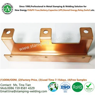
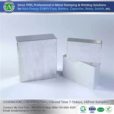
Our company has long been focusing on the R&D and manufacturing of PCB Bus Bars, which is widely used in power electronics, new energy and industrial control fields. We are committed to providing efficient and reliable copper busbar connection solutions for high-power PCB systems, and welcome exchanges and cooperation with colleagues in the industry.