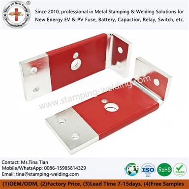
How can the issue of excessive inductance in EV film capacitor busbars be resolved?
Jul 27, 2026
The EV Film Capacitor Busbar serves as a critical interconnect component linking the inverter, electronic control system, and capacitor module in new energy vehicles, primarily facilitating high-frequency, high-current power transmission. Under high-frequency switching conditions-such as those involving SiC or IGBT technologies-excessive parasitic inductance in the busbar can trigger issues like voltage spikes, electromagnetic interference, and abnormal temperature rises. These problems directly compromise the operational stability and service life of the vehicle's electronic control system, making parasitic inductance a key parameter requiring strict control during the R&D and mass production of power electronics.

Main causes of excessive inductance
Flawed structural design is the primary cause of excessive inductance. Traditional non-laminated capacitor busbars suffer from issues such as excessive spacing between positive and negative terminals and overly long current paths; the failure to employ a scientifically engineered laminated design significantly increases the current loop area, resulting in persistently high parasitic inductance that fails to meet the operational requirements of high-frequency inverters.
Suboptimal interlayer structural design exacerbates the problem of excessive inductance. Laminated capacitor busbars rely on the tight bonding and lamination of copper and insulation layers to achieve low-inductance characteristics; however, in some products, disordered copper layer arrangements, loose coupling between positive and negative terminals, and poor interlayer layouts prevent effective magnetic field cancellation and fail to optimize current transmission paths, leading to consistently high overall inductance.
Deviations in mass production precision result in poor inductance consistency. During volume production, tolerance variations in copper thickness, stamping and bending dimensions, and insulation thickness can cause conductor misalignment and inconsistent interlayer spacing. A lack of dimensional precision leads to significant variations in inductance parameters between individual units, compromising the operational consistency of the busbar system.
Improper on-site installation practices amplify inductance-related issues. Suboptimal installation methods-such as excessively long connecting cables, an excessive number of external connection points, and disorganized terminal layouts-effectively lengthen the overall current transmission loop. This compounds the busbar's inherent parasitic inductance, leading to malfunctions such as voltage fluctuations and excessive interference during high-frequency IGBT operation.
Structural and Manufacturing Optimization Schemes for Inductance Reduction
Optimize the structural layout of laminated busbars to minimize parasitic inductance at the source. By reducing the spacing between positive and negative conductors, streamlining current transmission paths, and employing symmetrical conductor arrangements, the overall busbar layout is optimized; leveraging the principle of opposing currents in laminated layers reduces loop area and effectively suppresses parasitic inductance, making the design suitable for high-frequency power transmission in new energy applications.
Enhance mass production precision to ensure parameter consistency. Utilizing precision stamping and standardized bending processes, the thickness of copper conductors and insulation layers, as well as lamination alignment accuracy, are strictly controlled; this stabilizes conductor positioning, mitigates inductance fluctuations caused by manufacturing tolerances, and ensures uniform performance across mass-produced units.
Improve terminal structure and installation interface design. Minimize terminal connection distances, optimize mating points, and streamline external connection structures to reduce redundant current paths. Additionally, customize terminal configurations to match the dimensions of capacitors and inverters, thereby improving connection fit and reducing parasitic inductance introduced during installation.
Refine the performance verification and testing system for finished products. Conduct specialized testing on low-inductance busbars-covering parameters such as inductance, conduction resistance, insulation performance, and temperature rise cycling-to strictly monitor the core specifications of each batch, ensuring compliance with mass production standards for new energy power control equipment.

Our Manufacturing Advantages
To address issues such as excessive inductance, inconsistent structural uniformity, and performance fluctuations in mass production regarding busbars for new energy vehicle (NEV) capacitors, the company possesses comprehensive capabilities spanning from structural optimization to precision manufacturing. By employing processes such as precision stamping, accurate bending, laser welding, insulation lamination, and dimensional inspection, the company strictly controls conductor spacing, interlayer positioning, and insulation thickness, thereby minimizing parasitic inductance variations caused by manufacturing deviations.
Leveraging extensive experience in the electrical industry and adherence to the IATF16949 quality management system, the company provides customized development and mass production support for products such as EV Film Capacitor Busbar and laminated busbars. These solutions help customers optimize current paths and enhance electrical performance consistency, meeting the stringent requirements for low-inductance, high-reliability interconnects in NEV inverters, electronic control systems, and capacitor modules.
Contact Us
If you are developing electronic control systems, inverters, or capacitor modules for new energy vehicles and are facing issues such as excessive inductance in EV film capacitor busbars, voltage spikes, or connection reliability concerns, we invite you to discuss your specific application requirements. We offer comprehensive solutions tailored to different system architectures-ranging from design optimization and prototype development to mass production.