How To Solve Overheating Problems In Copper Stamping Parts?
Jul 28, 2026
Copper Stamping Parts serve as critical foundational components in electrical systems for new energy vehicles, battery systems, relays, and switchgear. Thanks to their excellent electrical conductivity, they are widely used in high-current electrical connection applications. However, during prolonged high-load operation, these parts frequently experience excessive temperature rises; this not only compromises electrical contact stability and shortens component lifespan but can also lead to circuit failures and threaten the operational safety of the entire electrical system. Such overheating issues-often stemming from design flaws, unstable stamping processes, or unreliable assembly connections-represent key challenges that must be rigorously addressed during engineering selection and manufacturing.

The primary cause of heating in copper stamped parts under high-current operating conditions.
Improper design and component selection are primary causes of overheating in stamped copper parts. Some products fail to align with actual current-carrying requirements during the R&D phase-suffering from insufficient conductive cross-sectional areas or inadequate material thickness-which leads to excessive current density per unit area. If the structure is not optimized based on electrical parameters, the part is highly susceptible to overheating due to overload. In engineering applications, the structural dimensions of the copper component must be optimized based on the equipment's maximum operating current; selecting appropriate copper materials and increasing the effective conductive area can resolve current-carrying capacity issues at the design stage.
Excessive contact resistance is a key trigger for localized overheating. Insufficient stamping precision can lead to flatness deviations; when combined with issues such as surface oxidation, plating defects, or unstable assembly pressure, this significantly increases contact resistance. High-precision stamping and standardized surface treatment processes can effectively optimize contact surface flatness. Furthermore, finishes such as tin, nickel, or silver plating can drastically improve contact surface conductivity, thereby mitigating the risk of overheating caused by contact resistance.
Manufacturing defects in the stamping process can lead to uneven current distribution and the formation of localized hotspots. Imperfections such as burrs, dimensional deviations, material deformation, and surface scratches compromise the integrity of the conductive path. High-precision progressive stamping processes ensure strict control over dimensional accuracy and surface quality, preventing manufacturing defects and guaranteeing consistent conductivity across all units, thereby eliminating localized overheating issues.
Poor heat dissipation design can also exacerbate temperature rise. In scenarios where installation space is cramped and surrounded by dense heat sources, a lack of heat dissipation considerations in the copper part's design prevents heat from escaping efficiently; long-term heat accumulation leads to a continuous rise in temperature. To address these conditions, heat dissipation efficiency can be improved by optimizing the product's structural geometry, adjusting the equipment layout, and allocating adequate space for heat dissipation, ensuring suitability for long-term, high-current operation.
Engineering Improvement Solutions and Key Points for Production Control
Scientific material selection is the foundation for temperature control and quality enhancement, as different copper alloys exhibit significant variations in electrical conductivity, strength, and thermal resistance. We flexibly select materials-such as pure copper and brass-based on specific equipment operating conditions. By precisely matching materials to environmental corrosion factors, current-carrying parameters, and structural strength requirements, we maximize the conductivity and heat dissipation advantages of copper while ensuring structural stability, making the parts suitable for a wide range of high- and low-voltage electrical equipment applications.
Precise control of the stamping process is essential for eliminating manufacturing defects. Our progressive die stamping service integrates the entire workflow-including custom die design, precision stamping, dimensional inspection, and rigorous burr control. Through standardized mass production management, we ensure consistent dimensional accuracy and structural flatness, eliminate conductivity anomalies caused by stamping flaws, and guarantee uniform performance across large production batches to meet the stable current-carrying needs of industrial equipment.
Specialized surface treatments provide a long-term solution to mitigate overheating risks. Processes such as gold, silver, nickel, and tin plating effectively remove surface oxidation layers and reduce contact resistance while enhancing oxidation and corrosion resistance. Leveraging a comprehensive surface treatment system, we significantly optimize electrical contact performance, minimize energy loss due to temperature rise during continuous operation, and extend the product's service life.
Rigorous electrical performance testing serves as the ultimate quality safeguard. During mass production, finished parts undergo resistance testing, temperature rise simulation, dimensional accuracy checks, and visual defect inspections. Through comprehensive performance verification, we identify products suitable for high-current applications and prevent substandard components from entering the assembly stage, thereby ensuring the stability of the equipment's electrical operation.

Manufacturing Capability for Reliable Copper Stamping Parts
The reliability of copper stamped parts depends not only on material selection but also on a comprehensive manufacturing system. Capabilities in stable mold development, precision stamping, electroplating, and inspection are crucial to ensuring product consistency.
In actual production, we leverage our in-house stamping workshops, mold development expertise, electroplating lines, and automated inspection equipment to maintain end-to-end control-from product design verification to mass production.
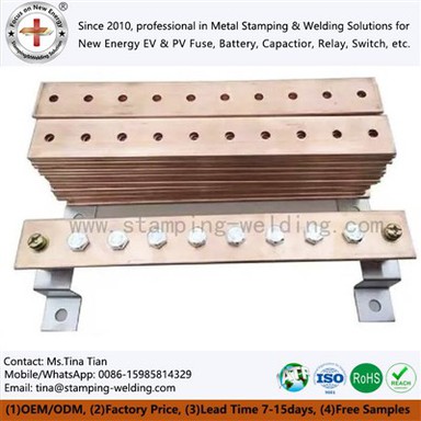
Furthermore, our multi-process manufacturing capabilities allow us to meet diverse application requirements; for instance, Copper Stamping Parts can be produced using a combination of stamping, welding, bending, and electroplating, providing complete solutions for new energy vehicles, electrical equipment, and industrial connection systems.
Adherence to quality management standards such as ISO9001, IATF16949, RoHS, and REACH ensures that our products meet international market requirements regarding safety, reliability, and environmental compliance.
Contact Us
If your Copper Stamping Parts encounter issues regarding temperature rise, contact stability, or structural design in high-current applications, we can provide material selection, structural optimization, and manufacturing support based on current parameters, installation environments, and product requirements to help enhance the reliability of electrical connections.