Fretting Corrosion in Electrical Contacts: Silver vs. Tin Electroplating Thickness Standards
Sep 25, 2026
Fretting corrosion occurs when two electrically conductive surfaces undergo small-amplitude relative motion under load, progressively disrupting the contact interface and increasing electrical resistance. For a silver-plated copper contact, the choice between silver and tin, combined with a specified plating thickness such as 3–10 μm, directly affects wear life, contact resistance stability, and exposure of the copper substrate.
For EV battery systems, ESS contactors, fuse assemblies, relays, power distribution units, and high-current busbars, plating should therefore be specified together with contact force, vibration amplitude, temperature cycling, substrate material, and inspection method rather than as an isolated coating thickness.

Fretting Wear Mechanism at 10–100 μm Amplitude Under IEC 60068-2-64 Vibration
Fretting begins when the apparent contact surfaces remain mechanically constrained while experiencing repeated micro-displacement. The displacement can be much smaller than the visible movement of the connector or busbar assembly.
At the microscopic interface, asperities repeatedly contact, deform, fracture, and oxidize. The resulting wear debris can accumulate between the conductive surfaces. When the contact force is insufficient to remove or penetrate this debris, the effective metallic contact area decreases, and contact resistance can increase.
For an electrical contact, the engineering sequence is generally:
Micro-motion → asperity deformation → coating wear → debris generation → substrate exposure → oxidation → resistance increase
IEC 60068-2-64 defines broadband random vibration testing for specimens exposed to stochastic vibration and allows accumulated mechanical degradation to be evaluated under specified test conditions.
Contact Force and 10–100 μm Micro-Motion Control
The severity of fretting is influenced by:
10–100 μm displacement: Small relative motion can repeatedly damage the contact interface without producing obvious macroscopic movement.
0.5–5 N contact force: The actual design value must be determined from contact geometry, current, vibration and mechanical retention requirements.
−40°C to +125°C thermal cycling: Differential thermal expansion can generate repeated interface movement even when external vibration is low.
IEC 60068-2-64 vibration: Random vibration can be used to reproduce accumulated mechanical degradation in vehicle and industrial electrical assemblies.
IATF 16949 process control: Contact force, plating thickness, substrate preparation, and dimensional tolerances should be linked to controlled manufacturing characteristics.
The relevant parameter is not simply whether a connector "moves." The engineering question is whether the local displacement repeatedly exceeds the elastic accommodation capability of the plated interface.
Copper Substrate Exposure at 3–10 μm Plating Thickness
A copper contact can provide high electrical conductivity, but exposed copper is not equivalent to a plated contact surface in a fretting environment.
When a silver or tin coating is locally removed, the resulting interface can contain copper oxides, transferred coating material, and mechanically generated debris. These products have different electrical properties from the original metallic contact surface.
For high-current applications, the plating system therefore needs to maintain:
stable metallic contact areas;
sufficient coating thickness after forming;
adhesion after stamping and bending;
resistance to mechanical wear;
controlled substrate exposure;
stable contact resistance after vibration and thermal cycling.
Silver vs. Tin Plating at −40°C to +125°C Thermal Cycling
Silver and tin do not behave identically under mechanical wear, oxidation, and temperature cycling. The correct selection depends on current level, contact force, environmental exposure, mating frequency, vibration, and the required electrical resistance stability.
| Parameter | Silver Plating | Tin Plating |
| Typical engineering use | High-current electrical contacts, busbars, contact assemblies | Terminals, connectors, lower-current interfaces |
| Electrical conductivity | Very high | Lower than silver |
| Fretting resistance | Generally favorable when properly specified | More sensitive to oxide/debris formation |
| Surface oxide behavior | Silver oxide has relatively low electrical impact compared with many base-metal oxides | Tin oxide can increase interface resistance |
| Thermal cycling | Suitable for high-temperature electrical interfaces when coating/substrate are properly controlled | Suitable when temperature and mechanical requirements are within coating specification |
| Typical thickness range discussed for engineering designs | 3–10 μm | 3–10 μm |
| Main design concern | Wear, sulfide exposure, adhesion, and coating uniformity | Fretting wear, oxide formation, and whisker control |
| Inspection | XRF thickness/composition, adhesion, visual inspection | XRF thickness/composition, adhesion, visual inspection |
| Relevant coating specification | ISO 4521:2008 | ISO 2093:1986 |
ISO 4521:2008 specifies requirements and test methods for electrodeposited silver and silver-alloy coatings used for electrical, electronic, and other engineering applications. The standard was reviewed and confirmed in 2023 and remains current.
Silver Plated Copper Contact at 3–10 μm
For high-current electrical contacts, silver plating provides a conductive surface over copper while maintaining the dimensional and conductivity advantages of the copper substrate.
A typical engineering specification can define:
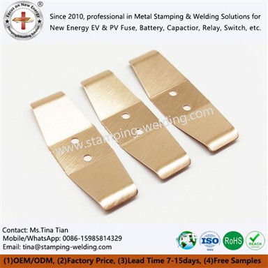
C1100 copper substrate: High-conductivity copper for current-carrying components.
3–5 μm silver plating: Suitable as a starting specification for applications with moderate mechanical wear.
5–10 μm silver plating: Used when greater wear allowance is required or when the contact surface experiences repeated mechanical stress.
±10–15% process control target: A practical internal process-control range may be established around the nominal thickness, subject to the customer's drawing and applicable coating specification.
XRF measurement: Non-contact thickness measurement without sectioning the finished component.
ISO 4521:2008: Reference specification for engineering silver and silver-alloy electrodeposits.
The 3–10 μm range should not be treated as a universal regulatory requirement. Final thickness must be established from contact load, expected displacement, wear allowance, corrosion environment, and product validation results.
Tin Plating at 3–10 μm and Fretting Risk
Tin remains widely used for electrical terminals because of its processability and cost structure. However, tin surfaces require greater attention to mechanical interface conditions.
Under repeated micro-motion, the tin layer can experience:
Surface deformation.
Wear debris generation.
Oxide accumulation.
Local coating thinning.
Increased constriction resistance.
Progressive exposure of the underlying copper.
For static connections with controlled contact pressure, tin can provide stable performance. For high-current interfaces exposed to repeated vibration and thermal expansion, the coating specification should be validated under the actual mechanical duty cycle rather than selected solely according to nominal thickness.
Silver vs. Tin: Engineering Selection at IEC 60068-2-64 Test Conditions
| Design condition | Silver-plated copper | Tin-plated copper |
| High-current busbar interface | Strong candidate | Requires application-specific validation |
| Repeated vibration | Suitable with controlled contact force and thickness | Requires fretting validation |
| High contact pressure | Suitable | Suitable within coating limits |
| Frequent mating cycles | Better suited to wear-resistant designs | Application dependent |
| −40°C to +125°C cycling | Requires thermal expansion analysis | Requires thermal expansion and oxide evaluation |
| 3 μm coating | May be adequate for low-wear interfaces | Requires validation |
| 5 μm coating | Common engineering starting point | Common engineering starting point |
| 10 μm coating | Increased wear allowance | Increased wear allowance but does not eliminate fretting mechanisms |
| High-current contactor | Frequently specified | Application dependent |
| XRF inspection | Applicable | Applicable |
The coating should be considered one layer of the electrical interface system. Contact geometry, spring force, substrate hardness, surface roughness, and mechanical retention remain equally important.
Request Free Contact Design Evaluation & Quote

3–10 μm Electroplating Thickness Control Under ISO 4521 and ISO 2093
Increasing plating thickness is not a substitute for correct contact mechanics. A 10 μm coating can still fail prematurely if the interface experiences excessive displacement, insufficient contact force, or poor adhesion.
Thickness should instead be treated as a controlled wear allowance.
3 μm vs. 5 μm vs. 10 μm Engineering Specification
| Nominal coating | Engineering purpose | Typical consideration |
| 3 μm | Basic conductive surface and limited wear allowance | Suitable only after application validation |
| 5 μm | Balanced conductivity and mechanical wear allowance | Practical starting point for many contact designs |
| 8 μm | Increased wear allowance | Useful for higher mechanical duty |
| 10 μm | High coating reserve | Requires process capability and dimensional review |
The actual acceptable range should be specified as a drawing requirement, for example:
Silver: 5.0 μm nominal, minimum local thickness ≥4.0 μm
or
Silver: 10 μm nominal, minimum local thickness ≥8.0 μm
The acceptance criterion must distinguish between average thickness, minimum local thickness, and thickness distribution.
Plating Thickness After Stamping and Bending at ±0.01 mm Tolerance
A common manufacturing error is to specify plating thickness without considering deformation.
For stamped copper contacts, the production sequence may be:
Copper strip → stamping → deburring → cleaning → activation → electroplating → rinsing → drying → inspection
Alternatively, pre-plated material may be stamped depending on the component geometry and required surface coverage.
Forming can influence:
coating cracking;
edge coverage;
local thickness;
burr exposure;
surface roughness;
contact flatness.
For precision stamped contacts with dimensional requirements such as ±0.01 mm, plating strategy should be incorporated into the tooling and tolerance stack-up.
Edge Coverage at 3–10 μm Plating Thickness
Sharp stamping edges are more difficult to plate uniformly than broad planar surfaces.
For high-current contacts, the engineering drawing should identify:
3–10 μm coating thickness: Required thickness range.
Contact zone: Functional plated area.
Non-functional zone: Area where coating thickness may be controlled differently.
Burr height: Controlled according to the electrical and mechanical interface.
Surface roughness Ra: Specified where contact resistance or mating wear requires it.
CMM inspection: Used to verify dimensional geometry after stamping and plating.
This approach prevents the common problem of meeting an average plating thickness while failing to maintain sufficient coating on the actual electrical contact zone.
XRF Thickness Measurement at 0.01–75 μm Measurement Capability
X-ray fluorescence provides a non-contact method for determining coating thickness and, depending on the coating system and instrument configuration, coating composition.
ASTM B568 describes X-ray spectrometry for measuring metallic and some non-metallic coating thicknesses. The method can cover approximately 0.01 μm to 75 μm, depending on the coating and substrate combination.
This makes XRF particularly useful for controlling 3–10 μm silver or tin coatings on copper contacts.
XRF Inspection at 3–10 μm Coating Thickness
A production inspection sequence can include:
ASTM B568: X-ray spectrometric coating-thickness measurement.
3–10 μm nominal thickness: Measurement range for the specified contact coating.
Multiple measurement points: Contact center, edge transition, and non-contact area.
XRF calibration: Reference standards matched to the coating/substrate combination.
CMM inspection: Dimensional verification after stamping and forming.
Visual inspection at 10×–50× magnification: Surface defects, discoloration, blistering, and exposed substrate.
Adhesion testing: Verification of coating integrity after forming and thermal exposure.
ASTM B568 also notes that the measured coating mass can be expressed as linear thickness when coating density is known.
Why XRF Is Preferred for Non-Destructive 3–10 μm Inspection
| Inspection method | Non-destructive | Suitable for production | Thickness information | Typical application |
| XRF | Yes | Yes | Local coating thickness | Silver/tin contact plating |
| Metallographic cross-section | No | Limited | Layer profile | Process validation |
| Micrometer | Yes | Yes | Total part dimension | Not coating-specific |
| Visual inspection | Yes | Yes | Surface condition only | Defect screening |
| Chemical stripping | No | Limited | Average coating amount | Laboratory verification |
For production control, XRF provides direct thickness data without cutting the contact.
For process validation, however, metallographic cross-sections can still be useful because they show coating morphology, interfacial condition, and localized defects that a single XRF measurement cannot fully characterize.

3–10 μm Plating Process Control from C1100 Stamping to XRF Inspection
A reliable Electroplated Busbar Supplier should control the entire process chain rather than treating electroplating as an isolated subcontracting operation.
C1100 Copper Stamping at ±0.01 mm Dimensional Control
For high-current contact components, C1100 copper provides high electrical conductivity and good forming characteristics.
The manufacturing sequence may include:
C1100 copper strip: High-conductivity current-carrying substrate.
Progressive die stamping: High-volume contact geometry production.
In-die riveting: Assembly of contact elements where required.
Deburring: Removal of mechanically generated burrs.
Ultrasonic or alkaline cleaning: Removal of oil and surface contamination.
Electroplating: Controlled silver or tin deposition.
XRF inspection: 3–10 μm coating verification.
CMM inspection: Geometry and positional tolerance verification.
IATF 16949 control plan: Process and inspection records linked to defined characteristics.
Electroplating Process Variables at 3–10 μm
Coating thickness depends on current density, plating time, bath chemistry, temperature, agitation, substrate preparation and component geometry.
A simplified relationship is:
Coating mass ∝ Current × Time × Current Efficiency
Actual thickness distribution additionally depends on local current density.
High-current-density edges can plate differently from recessed areas. Rack orientation and part spacing therefore influence thickness uniformity.
For this reason, a production specification should define the measurement location rather than relying on one nominal thickness value.
ASTM B568 XRF Sampling Plan for Production Lots
A production control plan can define:
| Control item | Example engineering requirement | Inspection method |
| Base material | C1100 copper | Material certificate |
| Plating | Ag or Sn | XRF composition |
| Nominal thickness | 3–10 μm | XRF |
| Minimum local thickness | Drawing-defined value | XRF |
| Dimensions | ±0.01 mm where required | CMM |
| Surface | No exposed substrate in contact zone | Visual + microscope |
| Adhesion | No peeling after specified test | Adhesion test |
| Vibration | Application-specific profile | IEC 60068-2-64 |
| Process system | IATF 16949 | Quality system audit |
The exact sampling frequency should be established through the customer's control plan, process capability and product risk analysis.
Request Free DFM Evaluation & Quote
Fretting Corrosion Validation at IEC 60068-2-64 and −40°C to +125°C
Plating thickness should be validated against the actual mechanical and environmental duty cycle.
A suitable validation program can combine vibration, thermal cycling, and electrical resistance monitoring.
IEC 60068-2-64 Random Vibration and Contact Resistance Monitoring
IEC 60068-2-64 addresses broadband random vibration and applies to specimens exposed to stochastic vibration environments, including vehicle-related applications.
For an electrical contact, the test program can monitor:
Initial contact resistance: Baseline value before environmental exposure.
Vibration exposure: Defined frequency spectrum and acceleration profile.
Thermal cycling: Example range of −40°C to +125°C where applicable.
Post-test resistance: Comparison against baseline.
Visual wear: Examination of the contact track.
XRF thickness: Confirmation of remaining coating.
Cross-section analysis: Verification of coating/substrate interface when required.
A coating that retains its nominal thickness but produces unstable electrical resistance under vibration has not necessarily met the functional requirement.
Contact Resistance and Thermal Rise at High Current
For a simplified resistive interface:
P = I²R
where:
P = contact power dissipation;
I = current;
R = electrical contact resistance.
At 200 A, increasing contact resistance from 50 μΩ to 100 μΩ changes the interface dissipation from:
P = 200² × 50 × 10⁻⁶ = 2 W
to:
P = 200² × 100 × 10⁻⁶ = 4 W
The electrical loss therefore doubles even though the absolute resistance change is only 50 μΩ.
This is why fretting corrosion must be treated as an electrical reliability problem rather than only a surface-finish problem.
Silver-Plated Copper Contact vs. Tin-Plated Copper Contact Selection at 200 A
For engineers specifying a silver-plated copper contact, the decision should be based on the complete operating envelope.
| Engineering factor | Silver-plated copper | Tin-plated copper |
| 100–200 A current path | Strong candidate | Requires thermal and resistance validation |
| High vibration | Suitable with validated interface mechanics | Requires fretting validation |
| 3 μm coating | Limited wear reserve | Limited wear reserve |
| 5 μm coating | Moderate wear reserve | Moderate wear reserve |
| 10 μm coating | Higher wear reserve | Higher wear reserve |
| −40°C to +125°C | Application-specific validation | Application-specific validation |
| Contact resistance stability | Generally favorable for high-current designs | Highly dependent on contact force and oxide control |
| Manufacturing inspection | XRF + dimensional inspection | XRF + dimensional inspection |
| Engineering coating reference | ISO 4521:2008 | ISO 2093:1986 |
No single coating thickness eliminates fretting. A 10 μm coating can provide greater material reserve than a 3 μm coating, but interface displacement, contact force, vibration spectrum, and environmental conditions remain determining factors.
IATF 16949 Quality Control for 3–10 μm Electroplated Contacts
For automotive and energy-storage supply chains, plating quality should be connected to incoming material control, process parameters, inspection records, and PPAP documentation.
PPAP Level 3 Documentation for Silver and Tin Plated Contacts
A typical submission package may include:
IATF 16949: Quality management system evidence where applicable.
PPAP Level 3: Dimensional results, material certifications, and process documentation.
DFMEA/PFMEA: Risk analysis for stamping and plating processes.
Control Plan: Defined coating, dimensional, and functional characteristics.
MSA: Measurement-system analysis for XRF and dimensional gauges.
Capability study: Cpk/Ppk evaluation for key dimensions and coating thickness.
Material certificate: Copper grade and temper verification.
Plating report: Silver or tin thickness and composition.
CMM report: Dimensional inspection.
Functional test: Contact resistance, thermal rise, or application-specific electrical validation.
ISO 4521 and ASTM B568 Traceability at 3–10 μm
The coating specification should identify:
Coating material + nominal thickness + minimum thickness + measurement method + measurement locations + acceptance criteria
For example:
Silver plating, 5.0 μm nominal, minimum local thickness ≥4.0 μm, XRF measurement according to ASTM B568, measurement points defined on engineering drawing.
This is more useful for production control than simply specifying "silver plated" or "5 μm silver."
ISO 4521 specifically covers engineering silver and silver-alloy electroplated coatings and associated test methods. ASTM B568 provides a non-destructive X-ray spectrometry method for coating-thickness measurement.
3–10 μm Coating Thickness Specification for OEM Electrical Contacts
A production drawing for a high-current contact should define the interface requirements with enough detail to prevent interpretation differences between the purchaser and supplier.
Recommended drawing fields include:
| Drawing characteristic | Example |
| Base metal | C1100 copper |
| Plating | Silver |
| Thickness | 5.0 μm nominal |
| Minimum local thickness | ≥4.0 μm |
| Measurement | XRF |
| Reference | ASTM B568 |
| Contact area | Defined on drawing |
| Dimensional tolerance | ±0.01 mm where applicable |
| Surface condition | No exposed substrate in functional zone |
| Contact resistance | Application-specific limit |
| Vibration | IEC 60068-2-64 profile |
| Quality documentation | PPAP Level 3 |
The supplier should also distinguish between plating before forming and plating after forming, because the manufacturing sequence affects edge coverage, deformation, and final coating integrity.
Engineering Conclusion: 3–10 μm Silver or Tin Requires Functional Validation
Fretting corrosion is controlled through the interaction of coating material, thickness, contact force, displacement, substrate, vibration, and temperature-not through coating thickness alone.
For high-current EV and ESS electrical interfaces, a silver-plated copper contact can be specified with a 3–10 μm engineering thickness range when supported by application validation. Tin can also be used where its mechanical, electrical, and environmental limits are acceptable.
For procurement, the most useful supplier specification is therefore not simply "silver or tin plated." It is a controlled combination of:
C1100/Cu substrate + plating chemistry + 3–10 μm thickness + defined minimum local thickness + XRF inspection + contact resistance validation + vibration testing + thermal cycling + PPAP documentation.
An Electroplated Busbar Supplier capable of controlling stamping, plating, XRF inspection, and functional validation under one quality system can reduce variation between the electrical design requirement and the delivered contact interface.
FAQ: 3–10 μm Plating, XRF and PPAP
What silver plating thickness should be specified for a high-current copper electrical contact?
A common engineering starting range is 3–10 μm, with 5 μm often used as a practical design point. The final nominal and minimum local thickness should be established from fretting displacement, contact force, current, environment, and validation results.
How is 3–10 μm silver or tin plating thickness measured without damaging the contact?
X-ray fluorescence (XRF) provides non-destructive coating-thickness measurement. ASTM B568 covers X-ray spectrometry for metallic coating thickness and can cover approximately 0.01–75 μm depending on the coating/substrate combination.
Can a silver-plated copper contact be supplied with PPAP Level 3 documentation?
Yes. A PPAP Level 3 package can include dimensional results, material certificates, XRF plating reports, process documentation, control plans, measurement-system analysis and functional test records according to the customer's submission requirements.
contact us