Nickel Barrier Layer Electroplating on Copper Contacts: Preventing Copper-Tin Intermetallic Diffusion
Nov 16, 2026
Copper contacts directly electroplated with tin can develop brittle Cu-Sn intermetallic compounds during prolonged exposure to temperatures above 100°C. These compounds increase interfacial brittleness and can contribute to Kirkendall void formation, contact degradation, and mechanical failure. Applying a controlled 2–5 μm nickel barrier layer between the copper substrate and tin coating reduces copper-tin interdiffusion and improves the thermal stability of electrical contacts.
Xiamen Apollo Stamping Welding Technology Co., Ltd. manufactures precision copper electrical contacts and electroplated metal components, with multi-layer Ni-Sn and Ni-Ag plating solutions for automotive relays, fuse contacts, switching devices, and industrial electrical assemblies.
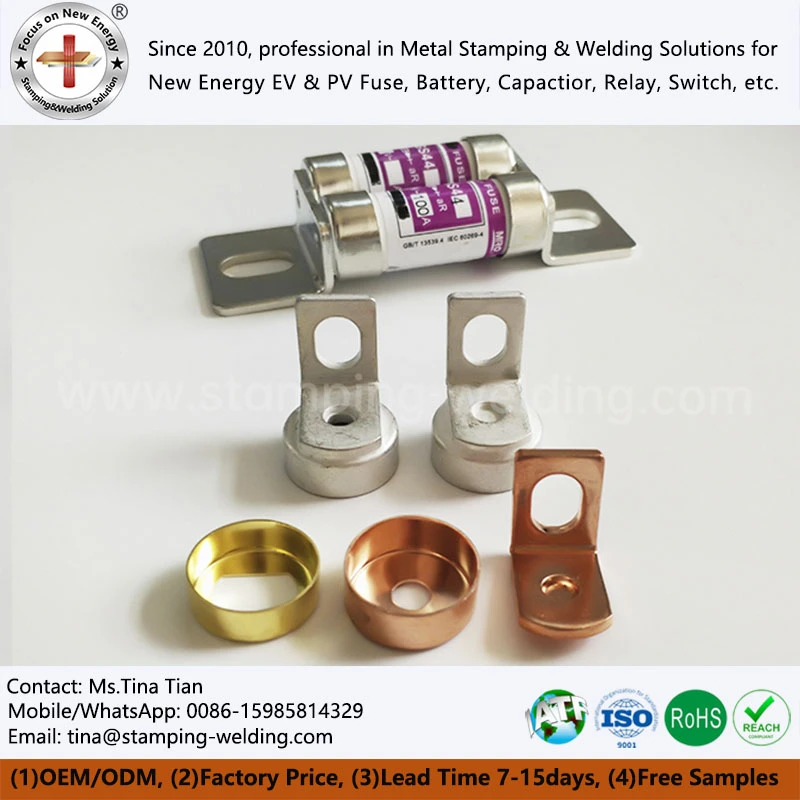
Copper-Tin Intermetallic Diffusion: Failure Mechanisms in High-Temperature Electrical Contacts
Why Direct Tin Plating on Copper Creates Reliability Risks Above 100°C
Tin electroplating is widely used on copper electrical contacts because of its solderability, relatively low contact resistance under suitable conditions, and corrosion protection.
However, copper and tin are not chemically inert at their interface. During thermal exposure, copper atoms diffuse into the tin layer while tin atoms diffuse toward the copper substrate. This interdiffusion produces Cu-Sn intermetallic compounds.
The principal reaction products include:
Cu₆Sn₅: commonly forms at the copper-tin interface.
Cu₃Sn: can develop between Cu₆Sn₅ and the copper substrate during continued aging.
The growth of these intermetallic layers changes the mechanical and electrical characteristics of the contact surface.
For electrical components operating above 100°C, prolonged thermal exposure can accelerate these reactions.
| Failure Mechanism | Physical Cause | Potential Electrical or Mechanical Consequence |
| Cu₆Sn₅ formation | Copper-tin interfacial reaction | Increased interfacial brittleness |
| Cu₃Sn growth | Continued solid-state diffusion | Reduced interface ductility |
| Kirkendall void formation | Unequal intrinsic diffusion fluxes | Interfacial porosity |
| Tin-layer consumption | Copper diffusion into tin | Reduced effective tin thickness |
| Interface degradation | Intermetallic growth and void accumulation | Increased cracking and delamination risk |
Kirkendall Void Formation and Interfacial Failure
The Kirkendall effect results from unequal diffusion rates of different atomic species across an interface.
In copper-tin systems, unequal intrinsic diffusion fluxes can produce a net vacancy flux. If vacancies are not sufficiently absorbed by sinks such as grain boundaries and dislocations, they may accumulate and form voids.
These voids can reduce the effective bonded area between the copper substrate and the plating layers.
Potential consequences include:
Reduced interfacial adhesion.
Increased susceptibility to thermal fatigue.
Localized stress concentration.
Coating delamination.
Unstable electrical contact performance.
The severity depends on the copper and tin microstructure, plating thickness, surface condition, temperature, and exposure duration.
Electrical Contact Reliability Under 150°C Thermal Exposure
Electrical contacts in automotive relays, fuse assemblies, and industrial switching equipment may experience repeated thermal loading.
The main reliability concern is not simply whether the initial tin coating passes visual inspection. It is whether the plated interface maintains its mechanical integrity and electrical performance after prolonged thermal exposure.
Relevant evaluation parameters include:
| Parameter | Initial Inspection | Post-Aging Evaluation |
| Tin coating thickness | XRF measurement | Remaining coating thickness |
| Nickel barrier thickness | XRF / cross-section | Barrier continuity |
| Intermetallic layer | Metallographic inspection | Cu-Sn layer growth |
| Adhesion | Initial adhesion test | Delamination and blistering |
| Contact resistance | Four-wire measurement | Resistance drift |
| Surface condition | Visual inspection | Oxidation and discoloration |
For high-temperature electrical contacts, a nickel diffusion barrier should be considered as part of the complete plating architecture rather than as an isolated coating operation.
2–5 μm Sulfamate Nickel Barrier: Mechanism for Suppressing Copper-Tin Interdiffusion
Nickel Barrier Layer as a Solid-State Diffusion-Controlled Interface
Nickel has a lower tendency to form the same Cu-Sn intermetallic phases at the copper-tin interface when used as an intervening barrier.
A properly deposited nickel layer separates the copper substrate from the outer tin coating, reducing direct atomic transport between copper and tin.
The typical plating architecture is:
The nickel layer acts as a kinetic barrier by reducing the rate of copper transport toward the tin coating.
The effectiveness of the barrier depends on:
Nickel thickness and uniformity.
Porosity and pinhole density.
Adhesion to the copper substrate.
Grain structure and deposit quality.
Plating bath stability.
Thermal exposure conditions.
A nominal thickness of 2–5 μm is a practical design range for evaluation, not a universal guarantee against diffusion. The final thickness must be validated against temperature, duration, contact geometry, and the required service life.
Why Sulfamate Nickel Electroplating Is Suitable for Precision Contacts
Nickel sulfamate electroplating is commonly selected when low internal stress and controlled deposit thickness are required.
Compared with some conventional nickel plating systems, sulfamate nickel baths can produce deposits with relatively low residual stress under properly controlled operating conditions.
| Process Characteristic | Sulfamate Nickel | Conventional Watts Nickel |
| Main nickel source | Nickel sulfamate | Nickel sulfate and nickel chloride |
| Internal stress | Can be controlled to relatively low levels | More dependent on bath chemistry and operating conditions |
| Deposit ductility | Generally suitable for ductile deposits | Depends on bath formulation |
| Thickness control | Suitable for precision deposition | Suitable with process control |
| Typical application | Engineering nickel deposits | Decorative and engineering applications |
| Process sensitivity | Bath composition and operating conditions | Bath composition and operating conditions |
For thin copper contacts, deposit stress is important because excessive internal stress may contribute to coating cracking, deformation, or adhesion problems.
Nickel Thickness Optimization: 2 μm vs. 5 μm
The nickel barrier must provide sufficient diffusion resistance without creating unnecessary electrical resistance or increasing manufacturing cost.
| Nickel Thickness | Engineering Characteristics | Typical Consideration |
| 2 μm | Lower material consumption | Requires strict porosity and continuity control |
| 3 μm | Intermediate barrier thickness | Suitable starting point for qualification |
| 5 μm | Greater diffusion-path thickness | Requires evaluation of contact resistance and geometry |
Request Free DFM Evaluation & Quote

High-Temperature Aging and Thermal Cycling Validation for Nickel-Plated Copper Contacts
150°C for 1,000 Hours: Accelerated Thermal Aging Test
High-temperature aging evaluates whether the nickel barrier maintains its diffusion-control function during prolonged exposure.
A proposed qualification condition for high-temperature electrical contacts is:
| Test Parameter | Proposed Test Condition |
| Aging temperature | 150°C |
| Exposure duration | 1,000 hours |
| Test environment | Controlled thermal chamber |
| Sample structure | Cu/Ni/Sn plated contact |
| Reference sample | Direct Cu/Sn plated contact |
| Primary analysis | SEM cross-section and EDS |
| Secondary evaluation | Adhesion and electrical resistance |
The direct Cu/Sn sample serves as a comparative reference to evaluate the effect of the nickel barrier.
Testing should include baseline measurements before aging and subsequent measurements at defined intervals.
Recommended inspection points include:
Nickel barrier continuity.
Cu₆Sn₅ and Cu₃Sn growth.
Kirkendall void distribution.
Tin-layer thickness retention.
Coating adhesion.
Electrical resistance variation.
The 150°C/1,000-hour condition is a proposed engineering qualification profile. It should not be interpreted as an automatic equivalent to a specific automotive lifetime or standardized service-life requirement.
Thermal Shock and Temperature Cycling
Static thermal aging does not fully represent the mechanical stresses generated by repeated temperature changes.
Copper, nickel, and tin have different coefficients of thermal expansion. Repeated heating and cooling can therefore generate cyclic interfacial stress.
Potential failure mechanisms include:
Nickel-tin interface cracking.
Copper-nickel adhesion degradation.
Coating blistering.
Interfacial fatigue.
Microcrack propagation.
A project-specific thermal cycling test should define:
| Test Variable | Required Definition |
| Minimum temperature | According to application requirements |
| Maximum temperature | According to application requirements |
| Dwell time | Defined for thermal stabilization |
| Temperature transition | Controlled chamber ramp rate |
| Cycle count | Customer qualification requirement |
| Electrical monitoring | Before and after cycling |
| Surface inspection | Blistering, cracking, and discoloration |
For automotive applications, the applicable customer specification or relevant environmental qualification standard should define the actual test profile.
SEM and EDS Verification of Nickel Barrier Integrity
Scanning Electron Microscopy (SEM) provides high-resolution imaging of the plated interface.
Energy Dispersive X-ray Spectroscopy (EDS) identifies the elemental distribution across the copper-nickel-tin structure.
The combined methods help establish:
1. Whether the nickel layer remains continuous.
2. Whether copper has penetrated the tin coating.
3. Whether tin has migrated toward the copper substrate.
4. Whether Cu-Sn intermetallic layers have developed.
5. Whether Kirkendall voids are present at the interface.
| Inspection Method | Primary Function | Evaluation Output |
| SEM | Interface morphology | Layer continuity and void distribution |
| EDS line scan | Elemental distribution | Cu, Ni, and Sn concentration profiles |
| Metallographic microscopy | Cross-sectional structure | Coating thickness and defects |
| XRF | Non-destructive coating thickness measurement | Ni and Sn thickness |
| Four-wire resistance | Electrical performance | Contact resistance variation |
| Adhesion test | Coating integrity | Peeling or separation behavior |
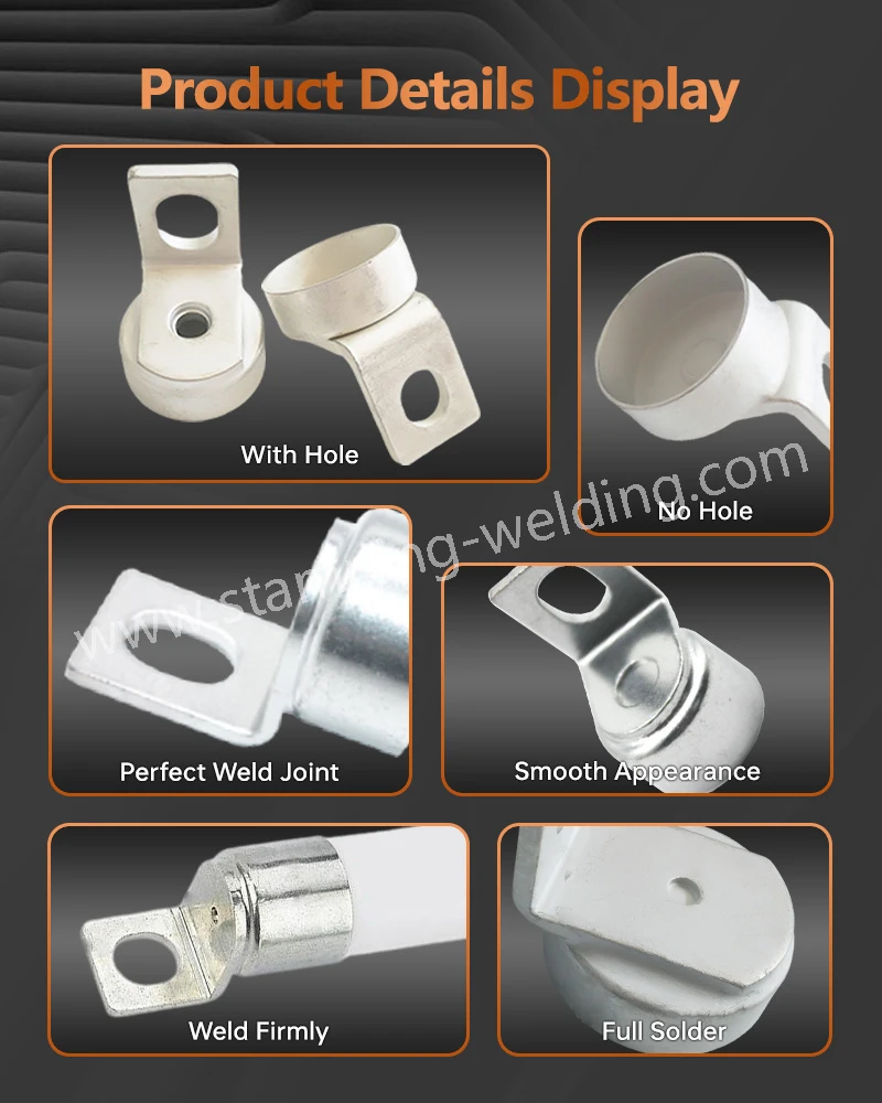
Electroplating Standards and Thickness Control: ASTM B733 and ISO 1456
Applying ASTM B733 and ISO 1456 to Nickel-Plated Copper Components
International plating standards provide requirements for coating classification, thickness, testing, and process acceptance.
However, ASTM B733 and ISO 1456 address different coating systems and should not be treated as interchangeable specifications.
| Standard | Scope | Relevance to Contact Plating |
| ASTM B733 | Autocatalytic (electroless) nickel-phosphorus coatings on metallic substrates | Relevant to electroless Ni-P barrier specifications |
| ISO 1456 | Electrodeposited nickel, nickel plus chromium, copper plus nickel, and related coatings | Relevant to applicable electrodeposited coating systems |
Important engineering distinction: Sulfamate nickel is an electrodeposited nickel process, whereas ASTM B733 addresses electroless nickel-phosphorus coatings. ASTM B733 should not be cited as the direct process standard for a sulfamate electroplated nickel layer.
For a Cu/Ni/Sn contact system, the drawing or plating specification should separately define:
Nickel deposition method.
Nickel thickness.
Tin coating thickness.
Coating locations and coverage.
Surface appearance.
Adhesion requirements.
Thermal aging acceptance criteria.
The applicable standard edition and coating classification should be confirmed during customer specification review.
XRF Coating Thickness Measurement and Cross-Section Verification
Nickel barrier thickness directly influences diffusion resistance. A coating that meets its average thickness target may still contain local thin regions or pores.
Apollo's inspection plan should combine non-destructive thickness measurement with destructive cross-section verification.
X-ray fluorescence (XRF)
Measures coating thickness without destroying the component.
Supports routine production inspection.
Provides local measurements at accessible locations.
Requires suitable calibration for the coating/substrate combination.
Metallographic cross-section
Measures individual layer thicknesses.
Reveals local discontinuities.
Identifies pores and interface defects.
Supports SEM/EDS characterization.
For small stamped electrical contacts, measurement location is particularly important because edges, corners, recesses, and narrow contact surfaces may receive different coating thicknesses.
Plating Defects and Process Prevention
| Plating Defect | Possible Root Cause | Preventive Control |
| Nickel pinholes | Surface contamination or poor deposition | Pretreatment and bath control |
| Uneven nickel thickness | Current-density distribution | Fixture and anode arrangement |
| Poor adhesion | Inadequate activation | Controlled cleaning and activation |
| Excessive internal stress | Bath imbalance | Sulfamate bath monitoring |
| Tin discoloration | Oxidation or contamination | Post-treatment and storage control |
| Edge burning | Excessive local current density | Current-density optimization |
| Plating blistering | Contamination or interfacial adhesion failure | Pretreatment verification |
The pretreatment sequence is particularly important for copper contacts.
A typical process sequence includes:
1. Alkaline degreasing.
2. Rinsing.
3. Acid activation.
4. Nickel electroplating.
5. Intermediate rinsing.
6. Tin electroplating.
7. Final rinsing.
8. Drying and inspection.
For nickel-silver systems, the plating sequence and interface preparation must be adjusted to the substrate, silver deposit specification, and application requirements.
Apollo Multi-Layer Electroplating for Precision Electrical Contacts
Ni-Sn and Ni-Ag Plating Systems for Electrical Components
Different electrical contact applications require different surface architectures.
Apollo's precision electroplating applications include nickel-tin and nickel-silver coating systems for copper-based electrical components.
| Plating Architecture | Layer Function | Typical Application |
| Cu/Ni/Sn | Nickel diffusion barrier with outer tin coating | Fuse contacts and electrical terminals |
| Cu/Ni/Ag | Nickel underlayer with silver contact surface | Relay and switching contacts |
| Cu/Sn | Direct tin plating | General electrical terminals |
| Cu/Ag | Direct silver plating | Electrical contact surfaces requiring silver |
The actual layer thickness, plating sequence, and surface treatment must be defined by the component drawing and application requirements.
Integration with Precision Metal Stamping
Electroplating quality depends on the condition of the stamped substrate.
Precision copper contacts may contain:
Blanking burrs.
Shear-edge deformation.
Residual stamping lubricant.
Surface scratches.
Localized forming stress.
These conditions influence cleaning efficiency, coating adhesion, and local current-density distribution.
A controlled manufacturing sequence integrates:
Precision stamping.
Deburring and surface preparation.
Degreasing and activation.
Multi-layer electroplating.
Coating thickness inspection.
Dimensional and functional verification.
For electrical contacts, the plating specification must also identify whether the contact surface, mating area, and non-functional regions require different coating coverage.
Production Quality Control and Automotive Documentation
For automotive relay and fuse contact programs, the supplier should establish a documented quality control plan.
Relevant deliverables include:
| Quality Document | Purpose |
| Material certificate | Verify copper substrate grade |
| Plating process specification | Define Ni-Sn or Ni-Ag architecture |
| XRF inspection report | Confirm coating thickness |
| Cross-section report | Verify layer structure |
| SEM/EDS report | Analyze diffusion and interface integrity |
| Adhesion test report | Confirm coating bonding |
| Thermal aging report | Evaluate high-temperature stability |
| PPAP documentation | Support automotive production approval |
Where required, PPAP Level 3 documentation can include process flow diagrams, PFMEA, control plans, dimensional results, material certifications, and performance validation reports.
The supplier's applicable IATF 16949 certification scope and customer-specific requirements should be confirmed before making automotive compliance claims.
Request Free DFM Evaluation & Quote
Design and Procurement Guidelines for Nickel-Plated Copper Contacts
Engineering Inputs Required for Electroplating Diffusion Barrier OEM Projects
To define the correct coating architecture, customers should provide:
Copper substrate grade, such as C1100 or C1020.
Base material thickness and contact geometry.
Operating temperature and expected exposure duration.
Required nickel barrier thickness.
Required outer tin or silver coating thickness.
Contact resistance limits.
Mechanical adhesion requirements.
Environmental and thermal cycling specifications.
These inputs determine whether a 2 μm, 3 μm, or 5 μm nickel barrier is suitable for the intended application.
Nickel Barrier Plating Selection Matrix
| Application Condition | Recommended Evaluation |
| General indoor electrical terminals | Direct tin plating may be sufficient |
| Continuous operation above 100°C | Evaluate Cu/Ni/Sn architecture |
| Long-duration exposure at 150°C | Perform 1,000-hour thermal aging qualification |
| High-current switching contacts | Evaluate contact resistance and temperature rise |
| Automotive relay components | Review PPAP and customer-specific qualification |
| Silver contact assemblies | Evaluate Cu/Ni/Ag interface and silver thickness |
A nickel barrier is not a substitute for correct contact design. Contact force, surface finish, current density, environmental exposure, and mating-material compatibility remain independent reliability factors.
Frequently Asked Questions
1. What nickel thickness is recommended for preventing copper-tin intermetallic diffusion?
A 2–5 μm sulfamate nickel layer is a practical starting range for qualification. The final thickness must be established through coating continuity inspection, thermal aging, and SEM/EDS analysis under the specified operating conditions.
2. How do manufacturers verify nickel diffusion barrier performance after 150°C aging?
Manufacturers use controlled thermal aging followed by SEM cross-section analysis, EDS elemental mapping, XRF thickness measurement, adhesion testing, and four-wire contact resistance measurement to evaluate barrier integrity.
3. Can nickel-plated copper contacts meet automotive PPAP Level 3 requirements?
Yes. A qualified supplier can prepare PPAP Level 3 documentation covering material certification, plating specifications, dimensional inspection, process control, coating thickness, adhesion, and customer-required thermal validation.
contact us