Progressive Die Engineering Secrets: Achieving ±0.01mm Tolerances in Precision Copper Terminals
Oct 03, 2026
Precision copper terminals requiring ±0.01mm dimensional tolerance depend less on final inspection than on progressive die architecture, material control, and in-process monitoring. For high-volume Precision Progressive Die Stamping, die clearance, carbide punch geometry, multi-stage bending, strip guidance, and sensor feedback must be designed as one controlled system.
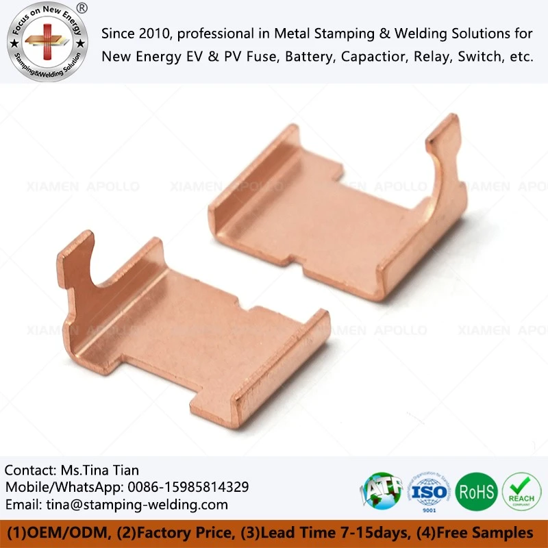
For EV battery terminals, power-electronics connectors, relay components, and high-current electrical contacts, dimensional drift can increase contact resistance, disturb assembly force, or create misalignment during automated insertion. A high-precision copper stamping OEM therefore needs to control the forming process at the die rather than attempt to correct variation after stamping.
±0.01mm Precision Starts with Terminal Stamping Tooling Design
A progressive die converts coil stock into a finished terminal through sequential piercing, blanking, coining, forming, bending, and cut-off operations. At a ±0.01 mm tolerance, every station contributes to the final dimensional stack-up.
The die design should establish a fixed datum system before individual station geometry is developed. Functional dimensions should reference the same strip datum wherever possible rather than accumulating tolerances from preceding bends or holes.
IATF 16949 datum control for ±0.01mm terminal stamping
A practical datum architecture separates the terminal into three control groups:
Primary datum: carrier strip or locating feature controlling strip pitch.
Secondary datum: pilot hole or precision-pierced feature controlling longitudinal position.
Functional datum: terminal contact, mounting hole, or mating surface controlled against the assembly requirement.
For high-precision copper stamping, typical process targets include:
| Parameter | Engineering Target | Primary Control |
| Finished critical dimension | ±0.01mm | Die geometry + CMM |
| Strip pitch | ±0.01–0.02mm | Pilot system |
| Hole diameter | ±0.01mm | Carbide punch/die clearance |
| Burr height | Process-specific | Punch edge + clearance |
| Bend angle | ±0.5° or tighter | Multi-stage forming |
| Material thickness | Supplier specification | Incoming inspection |
| Die alignment | Micron-level process control | Die maintenance + guide system |
| Final dimensional verification | CMM | PPAP Level 3 documentation |
The critical point is that ±0.01mm should not be treated as a final inspection specification alone. If the process capability cannot maintain the dimension during continuous production, sorting finished parts does not constitute process control.
C1100 and C2680 material behavior under IATF 16949 control
Copper terminals are sensitive to both material thickness and mechanical properties. C1100 pure copper offers high electrical conductivity, while C2680 brass provides greater strength and different forming behavior.
| Property | C1100 Pure Copper | C2680 Brass |
| Primary advantage | High electrical conductivity | Higher mechanical strength |
| Typical application | High-current terminals, busbar interfaces | Connector terminals, structural contacts |
| Forming behavior | High ductility; deformation can increase springback variation | Higher strength; greater forming force |
| Conductivity | Up to approximately 100% IACS depending on condition | Lower than pure copper |
| Tooling consideration | Adhesion and galling control | Higher forming load |
| Surface requirement | Electrical contact applications may require plating | Tin/nickel plating commonly used |
Material certification should be correlated with coil lot, temper, thickness, and stamping direction. A material substitution that appears dimensionally equivalent on a drawing can change forming force and springback.
Request Free DFM Evaluation & Quote
Carbide Punches and SKD11 Die Steel: IATF 16949 Tool Life Engineering
Punch material directly affects edge stability, burr formation, dimensional repeatability, and maintenance intervals. For copper terminals requiring long production runs, the choice between hardened SKD11 and carbide should be based on load, geometry, material condition, and expected stroke count.
Tungsten carbide vs SKD11 for high-precision stamping
| Tool Material | Typical Characteristics | Precision Application | Main Risk |
| Tungsten carbide | Very high hardness and wear resistance | Fine piercing, narrow slots, critical holes | Brittle under impact or misalignment |
| SKD11 | High hardness, toughness, machinability | General punches, dies, forming inserts | Edge wear over long runs |
| Carbide + SKD11 combination | Wear-resistant cutting with tougher support | High-volume progressive dies | Requires controlled assembly |
| Coated tool steel | Reduced friction and improved wear behavior | High-speed production | Coating damage if substrate is unstable |
For fine terminal piercing, carbide punches can maintain a sharper cutting edge over extended production. However, carbide should not be selected simply because it is harder.
A poorly aligned carbide punch can fracture where an SKD11 punch would deform or wear gradually.
1. Die clearance controls burr height and dimensional stability
Copper has high ductility and can produce undesirable rollover, burr, or secondary deformation when clearance is poorly matched to material thickness.
The effective clearance depends on:
Copper alloy and temper
Material thickness
Punch geometry
Cutting speed
Required burr height
Hole diameter
Expected tool life
For a high-precision terminal, the die clearance must be validated experimentally rather than copied from a generic percentage table.
A production trial should correlate:
clearance → cutting force → fracture zone → burr height → dimensional deviation → tool wear
This creates a measurable process window for subsequent die maintenance.
2. SKD11 support structures reduce carbide fracture risk
Carbide inserts should be mechanically supported rather than exposed to uncontrolled lateral loading. Precision progressive dies commonly combine carbide cutting components with hardened tool-steel holders, guide structures, and replaceable inserts.
The objective is not simply maximum hardness. The objective is controlled load transmission.
Multi-Stage Bending and Springback Control for ±0.01mm Terminals
Bending is often the largest source of dimensional variation after piercing. A terminal can leave the cutting station within tolerance and still fail final inspection because elastic recovery changes its angle or functional height.
Springback is affected by:
Material yield strength
Work-hardening behavior
Bend radius
Material thickness
Grain direction
Forming angle
Tool radius
Number of forming stages
Contact pressure
Tool wear
Multi-stage forming reduces angular variation under IATF 16949 control
A high-precision progressive die should avoid forcing a severe bend into a single station whenever the final geometry is sensitive to springback.
A typical sequence may use:
Pre-forming: establish the initial bend geometry.
Intermediate forming: increase the bend angle while distributing plastic deformation.
Calibration forming: establish the final functional angle.
Coining or restrike: stabilize critical surfaces where required.
Final inspection: verify the functional datum using CMM or dedicated gauges.
| Forming Strategy | Springback Control | Tool Load | Dimensional Repeatability |
| Single-stage bending | Limited | High local load | Lower |
| Two-stage bending | Improved | Distributed | Improved |
| Three-stage forming | High control | Distributed | High |
| Forming + restrike | Very high for selected features | Higher final load | High |
| Coining | Strong local deformation control | High | High for controlled features |
The number of stations should be determined from material behavior and geometry rather than from a fixed tooling template.
Bend compensation should be built into the die
If a terminal requires a final angle of 90°, the forming punch should not necessarily be designed around a nominal 90° tool position.
The actual process may require over-forming, followed by controlled elastic recovery.
For production validation, the engineering team should record:
Tool angle
Actual stamped angle
Springback angle
Material lot
Strip direction
Tool stroke
Production stroke count
This creates a traceable relationship between tooling geometry and finished-part variation.
In-Die Sensors for Real-Time Process Control and PPAP Level 3
A progressive die operating at high stroke rates cannot depend entirely on end-of-line inspection. A damaged punch, missing component, feeding error, or double strip can produce hundreds of defective parts before the operator detects the problem.
In-die sensors convert selected process conditions into immediate production signals.
Sensor-controlled progressive stamping under PPAP Level 3
Common monitoring points include:
Material presence
Strip position
Pilot engagement
Part presence
Misfeed detection
Double material detection
Punch breakage
Ejection confirmation
Die overload
Forming position
| Sensor Function | Detectable Condition | Production Risk if Uncontrolled |
| Strip sensor | Material missing | Empty stroke |
| Pilot sensor | Incorrect strip position | Hole/bend misalignment |
| Part sensor | Part not ejected | Die obstruction |
| Punch monitoring | Punch damage | Burr or dimensional failure |
| Load monitoring | Abnormal forming force | Tool damage |
| Feed monitoring | Incorrect pitch | Station misregistration |
| Double-sheet detection | Material overlap | Punch fracture |
For PPAP Level 3, the sensor strategy should be connected to the process FMEA, control plan, MSA activities, and dimensional validation.
The sensor itself is not the quality system. Its value comes from linking the signal to a defined reaction plan.
Process capability should accompany ±0.01mm specifications
For a critical terminal dimension, Cp and Cpk should be calculated from production data rather than assumed from a prototype run.
Where:
USL = upper specification limit
LSL = lower specification limit
μ = process mean
σ = standard deviation
If the specification is ±0.01mm, the total tolerance width is only 0.02mm. Small changes in material thickness, tool wear, strip alignment, or forming force can therefore consume a significant portion of the available process window.
CMM Inspection and IATF 16949 Traceability for Precision Copper Stamping
A coordinate measuring machine should not be used only as a final acceptance tool. CMM data can also support die tryout, first-off approval, preventive maintenance, and engineering change validation.
CMM measurement strategy for ±0.01mm terminals
Critical characteristics should be divided into:
Hole position
Hole diameter
Overall length
Terminal width
Bend height
Bend angle
Contact position
Flatness
Formed profile
A CMM program should reproduce the functional datum structure defined in the engineering drawing.
For example, measuring a terminal height against an unstable outer edge can produce a technically accurate measurement that does not represent the actual assembly condition.
The inspection method must therefore correspond to the product's functional datum scheme.

Progressive Die Maintenance: Controlling Tool Wear After 1 Million Strokes
Tooling consistency is not static. Cutting edges wear, forming surfaces polish, clearances change, and guide components gradually lose their original condition.
For high-volume copper terminal production, preventive maintenance should be based on measurable process indicators rather than an arbitrary calendar interval.
Tool-life monitoring under IATF 16949 process control
Track at minimum:
Production stroke count
Burr height
Critical hole diameter
Critical hole position
Bend angle
Forming height
Stamping force
Sensor alarm frequency
Punch replacement history
Grinding allowance
A useful maintenance trigger can be established when a process indicator approaches its control limit.
For example:
stroke count → burr growth → hole dimension drift → Cpk reduction → punch maintenance
This is more informative than stating that a die has a theoretical "million-shot life."
Tool life depends on material, thickness, geometry, lubrication, stroke rate, die clearance, and maintenance practice.
Die maintenance should preserve the original datum system
After grinding or replacing a punch, the restored component must maintain its relationship with:
Pilot system
Guide post
Die insert
Strip carrier
Adjacent forming station
Replacing a single worn component without checking the complete station can introduce a new dimensional offset.
Engineering Selection Matrix: ±0.01mm Copper Terminal Production
The following matrix summarizes the relationship between product requirements and tooling decisions.
| Product Requirement | Recommended Engineering Control | Verification |
| ±0.01mm hole dimension | Carbide punch + controlled clearance | CMM |
| High-volume piercing | Carbide cutting components | Burr measurement |
| Complex terminal geometry | Multi-stage forming | Profile/CMM |
| Sensitive bend angle | Pre-form + calibration/restrike | Angle gauge/CMM |
| High electrical conductivity | C1100 copper | Material certificate + conductivity test |
| Higher structural strength | C2680 brass | Material certificate + mechanical data |
| Continuous high-speed production | In-die sensors | Sensor validation |
| Automotive Tier 1 supply | IATF 16949 process system | Audit + PPAP |
| New tooling approval | Full dimensional validation | PPAP Level 3 |
| Long production run | Preventive tool maintenance | Stroke/tool-life records |
Download Stamping Design Specification
From DFM to PPAP Level 3: What a Production-Ready Die Must Control
A precision stamping project should begin with the part drawing and functional requirements rather than with a standard die configuration.
During DFM review, the engineering team should examine:
Material grade and temper
Strip thickness
Grain direction
Minimum bend radius
Hole-to-edge distance
Burr direction
Piercing sequence
Carrier design
Strip pitch
Progressive station allocation
Forming load
Scrap evacuation
Sensor locations
Inspection datums
Surface treatment requirements
For EV and ESS electrical components, electrical performance should also be considered during mechanical design.
A terminal dimension that meets ±0.01mm may still be unsuitable if plating thickness, contact force, mating geometry, or current-carrying cross-section is outside specification.
For this reason, mechanical dimensional control and electrical validation should be reviewed together.
PPAP Level 3 documentation should connect tooling to production control
A production submission can include:
Process Flow Diagram
PFMEA
Control Plan
MSA
Dimensional Results
Material Certifications
Capability Studies
Tooling Records
Process Parameters
Appearance Approval
Functional Test Results
Sample Parts
Part Submission Warrant
The purpose is to demonstrate that the manufacturing process-not simply a selected batch of parts-can repeatedly meet the drawing requirements.
Precision Progressive Die Stamping for EV and ESS Copper Terminals
For high-current electrical terminals, precision stamping is a controlled interaction between material behavior, die geometry, forming sequence, tooling materials, machine accuracy, and inspection.
A high-precision copper stamping OEM targeting ±0.01mm should establish the process around four engineering controls:
Terminal Stamping Tooling Design based on functional datums and controlled tolerance stack-up.
Carbide and SKD11 tooling selection matched to cutting load, wear, geometry, and maintenance requirements.
Multi-stage bending and calibration to control springback rather than relying on single-stage forming.
In-die sensor monitoring and CMM inspection to detect process drift before large quantities become nonconforming.
For automotive and energy-storage programs, these controls can then be integrated with IATF 16949, PPAP Level 3, process capability studies, and documented tool-life management.
The result is not simply a stamped copper terminal that passes inspection. It is a stamping process with measurable relationships between material → tooling → forming → inspection → process capability → production repeatability.
FAQ: Precision Copper Terminal Stamping
How can a progressive die maintain ±0.01mm tolerance during high-volume copper terminal production?
Use a controlled datum system, precision carbide tooling, validated die clearance, multi-stage forming, in-die sensors, preventive maintenance, and CMM-based process verification. Material thickness and temper must also remain within the approved specification.
What tooling materials are used for high-precision copper terminal stamping?
Tungsten carbide is commonly used for high-wear cutting components and critical piercing operations, while SKD11 is used for punches, dies, holders, and forming components where greater toughness and serviceability are required.
Can a copper terminal stamping supplier provide PPAP Level 3 documentation?
Yes. A production-ready program can include dimensional reports, PFMEA, control plan, MSA, capability studies, material certificates, process flow, tooling records, sample parts, and Part Submission Warrant documentation.
contact us